

Semiconductor Device
a technology of semiconductor devices and electromagnetic waves, applied in the field of semiconductor devices, can solve the problems of reducing the amplitude of electromagnetic waves emitted from the reader/writer, the communication distance is reduced, and the use of electromagnetic waves may occur, so as to prevent the reduction of electromagnetic waves, prevent the heating of the element forming layer, and suppress the current
- Summary
- Abstract
- Description
- Claims
- Application Information
AI Technical Summary
Benefits of technology
Problems solved by technology
Method used
Image

Examples
embodiment mode 1
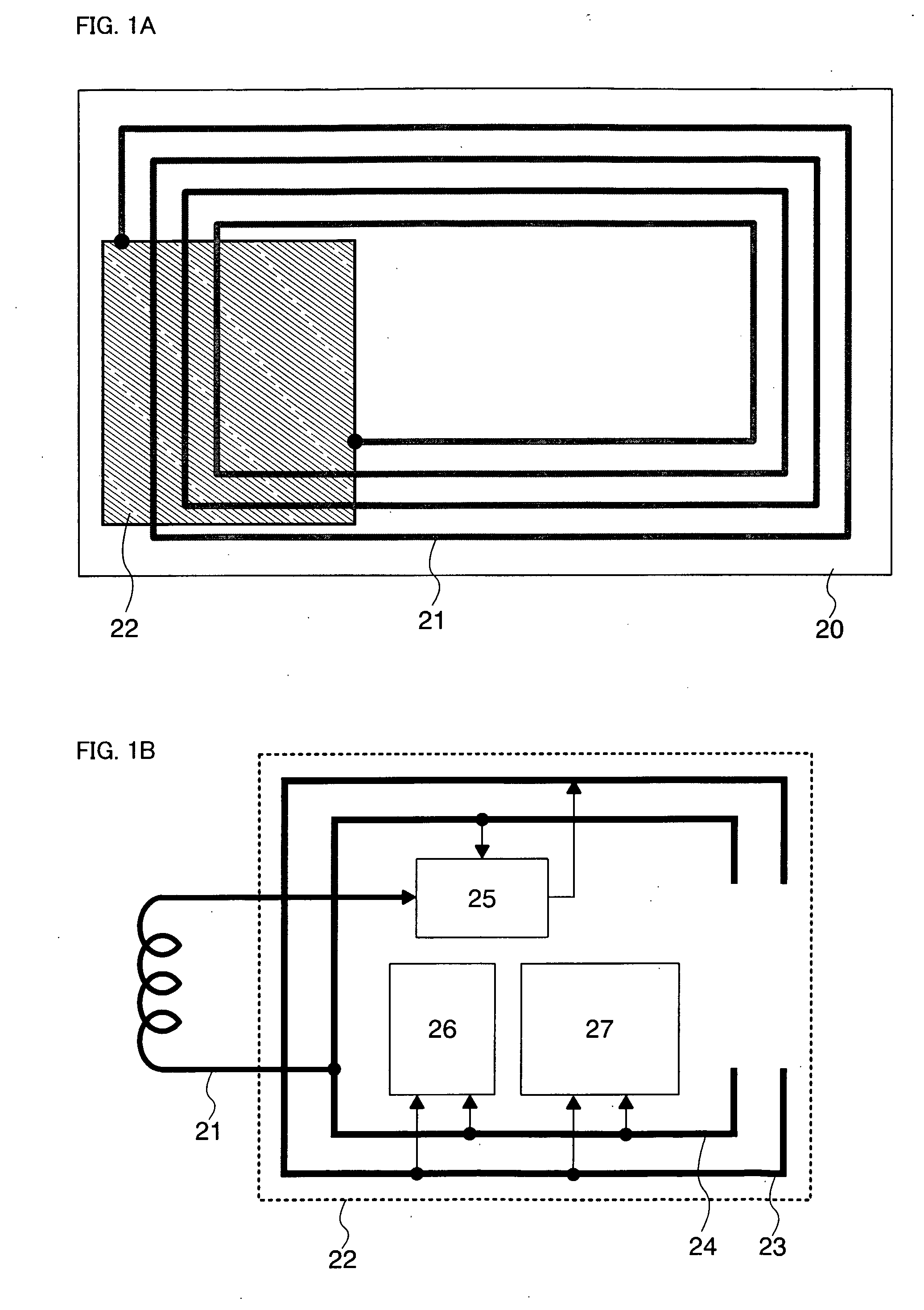
[0027] A configuration example of a semiconductor device of the invention is described with reference to FIGS. 1A and 1B. Note that FIG. 1A is a top plan view of the semiconductor device while FIG. 1B is a schematic view of an element forming layer in the semiconductor device.
[0028] As shown in FIG. 1A, the semiconductor device shown in this embodiment mode has an element forming layer 22 and an antenna 21, which are formed over a substrate 20. The element forming layer 22 and the antenna 21 may be arranged in any shape; however, they are preferably arranged so as to overlap each other in view of the reduction in size of the semiconductor device. If the antenna 21 is arranged in a coil, the element forming layer 22 is preferably arranged so as to overlap the end of the antenna 21. This is to prevent the amplitude of electromagnetic waves passing through the antenna 21 from being reduced by disposing the element forming layer 22 at the center of the antenna 21.
[0029] The substrate ...
embodiment mode 2
[0037] In this embodiment mode, a structure example of the semiconductor device, which is different from that shown in the aforementioned embodiment mode, is described with reference to drawings.
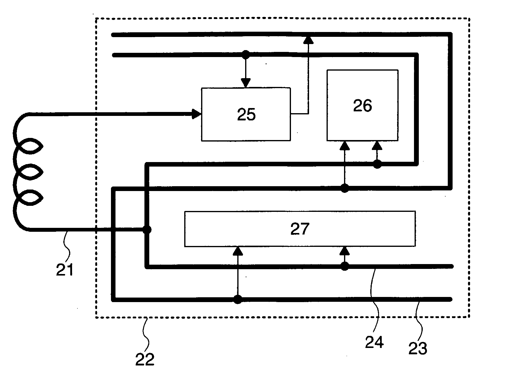
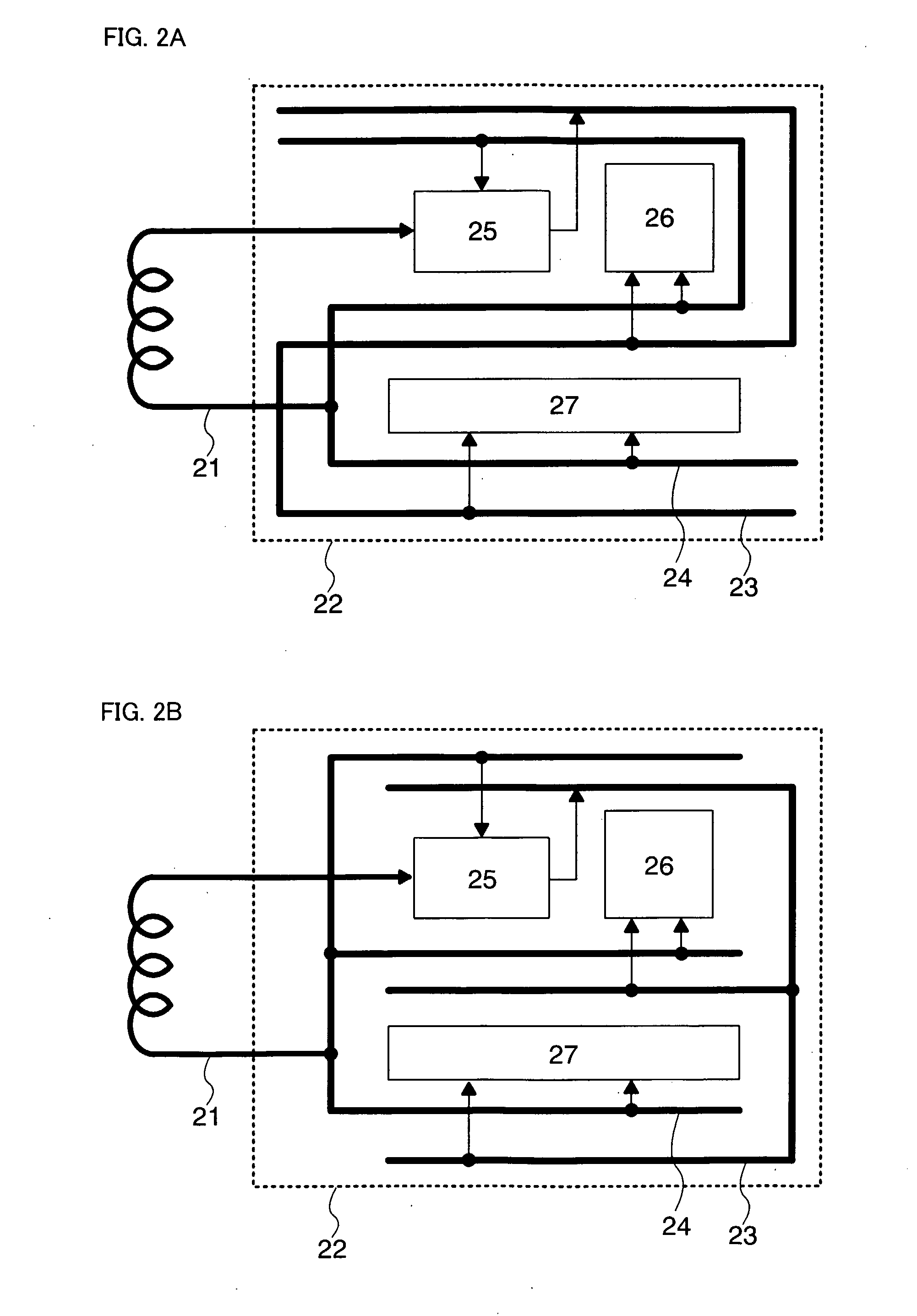
[0038] Described in the aforementioned embodiment mode is an example where wires such as a power supply wire and a ground wire, which are arranged in a circular shape so as to surround functional circuits and the like, are partially cut off to be formed into a U-shape. However, the invention is not limited to this, and wires such as a power supply wire and a ground wire may be arranged in any shape as long as it is not influenced by a change in a magnetic field. Specific examples different from that shown in the aforementioned embodiment mode are described below with reference to the drawings.
[0039] In FIGS. 2A and 2B, the power supply wire 23 and the ground wire 24 are provided so as to pass between the power supply circuit 25 and the functional circuits 26 and 27. In FIG. 2A, the power s...
embodiment mode 3
[0046] In this embodiment mode, an example of manufacturing steps of the semiconductor device of the invention is described with reference to drawings. Specifically shown is an example of manufacturing a semiconductor device using a thin film transistor (TFT) as a transistor on an element forming layer by a separating method where a TFT is provided over a support substrate and then separated therefrom.
[0047] First, a separation layer 702 is formed over a surface of a substrate 701 (FIG. 6A). The substrate 701 may be a glass substrate, a quartz substrate, a metal substrate such as stainless having a surface over which an insulating film is formed, a plastic substrate having heat resistance to the processing temperature of the steps, or the like. Such a substrate 701 has no limit in terms of size and shape. Accordingly, for example, if a rectangular substrate with each side of one meter or more is used for the substrate 701, productivity can be dramatically increased. This is a major...
PUM
 Abstract
Description
Claims
Application Information