Charge Domain Filter Device

a filter device and charge domain technology, applied in the field of filter devices, can solve the problems of sinc filter circuits unsuitable for filtering a wideband signal, signal degradation,

Inactive Publication Date: 2008-04-17
SONY CORP
View PDF5 Cites 18 Cited by
  • Summary
  • Abstract
  • Description
  • Claims
  • Application Information

AI Technical Summary

Benefits of technology

[0016] In view of the above, the present invention provides a charge domain filter device capable of filtering a signal without producing significant degradation in high-frequency components of the signal.
[0018] In this charge domain filter device, the SINC filter is configured to have the frequency characteristic expressed by a SINC function, and the bandpass is configured to have the frequency characteristic with the particular center frequency such that the charge domain filter device can pass a signal without producing significant degradation in a high-frequency component of the signal.
[0019] The bandpass filter may subtract a part of a previous sampled output signal from a current sampled output signal in synchronization with a clock of the SINC filter. That is, in this configuration, the bandpass filter subtracts a part of the previous sampled output signal from the current sampled output signal so that the bandpass filter functions as an IIR filter operable with low power consumption.
[0020] The SINC filter may include a first SINC filter adapted to provide the current sampled output signal, and a second SINC filter adapted to provide the previous sampled output signal, whereby the SINC filter is adapted to sample a differential signal. In this configuration, the first SINC filter is adapted to provide the current sampled output signal, and the second SINC filter is adapted to provide the previous sampled output signal, thereby making it possible for the SINC filter to sample a differential signal.
[0026] As described above, the present invention provides an advantage that the charge domain filter device can filter a signal without producing significant degradation in a high-frequency component of the signal.

Problems solved by technology

That is, when a signal is passed through the SINC filter circuit, signal degradation occurs in high-frequency components of the signal, and thus the SINC filter circuit is unsuitable for use for filtering of a wideband signal.

Method used


Image

  • Charge Domain Filter Device
  • Charge Domain Filter Device
  • Charge Domain Filter Device

Examples


first embodiment

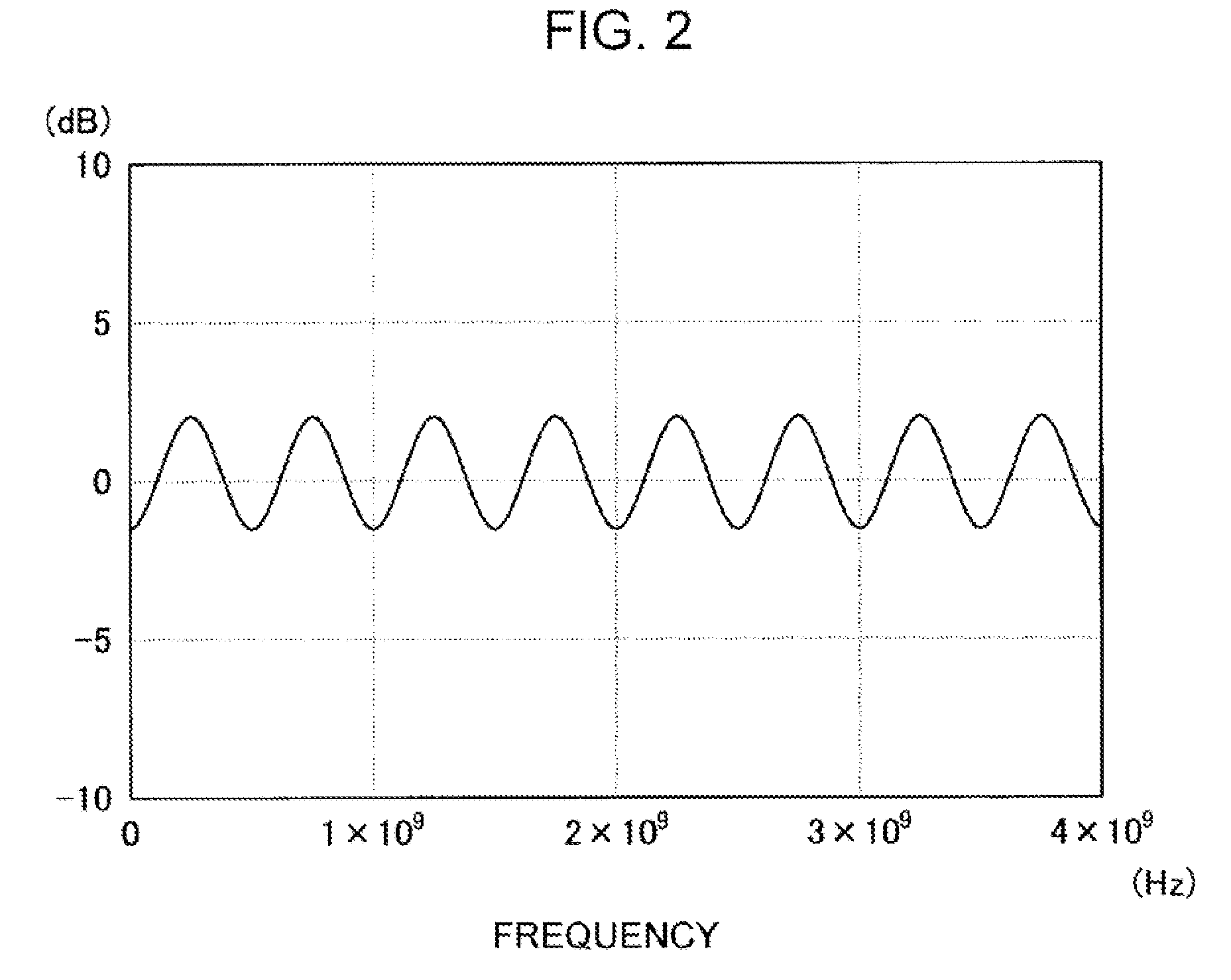
[0040] According to a first embodiment of the present invention, a charge domain filter circuit operable without producing degradation in high-frequency components of a signal is realized by connecting a BPF (Band-Pass Filter) to an output end of a SINC filter circuit according a conventional technique whereby the frequency characteristic of the SINC filter circuit is compensated for by the BPF so as to achieve a flat frequency characteristic over a range up to ¼t.

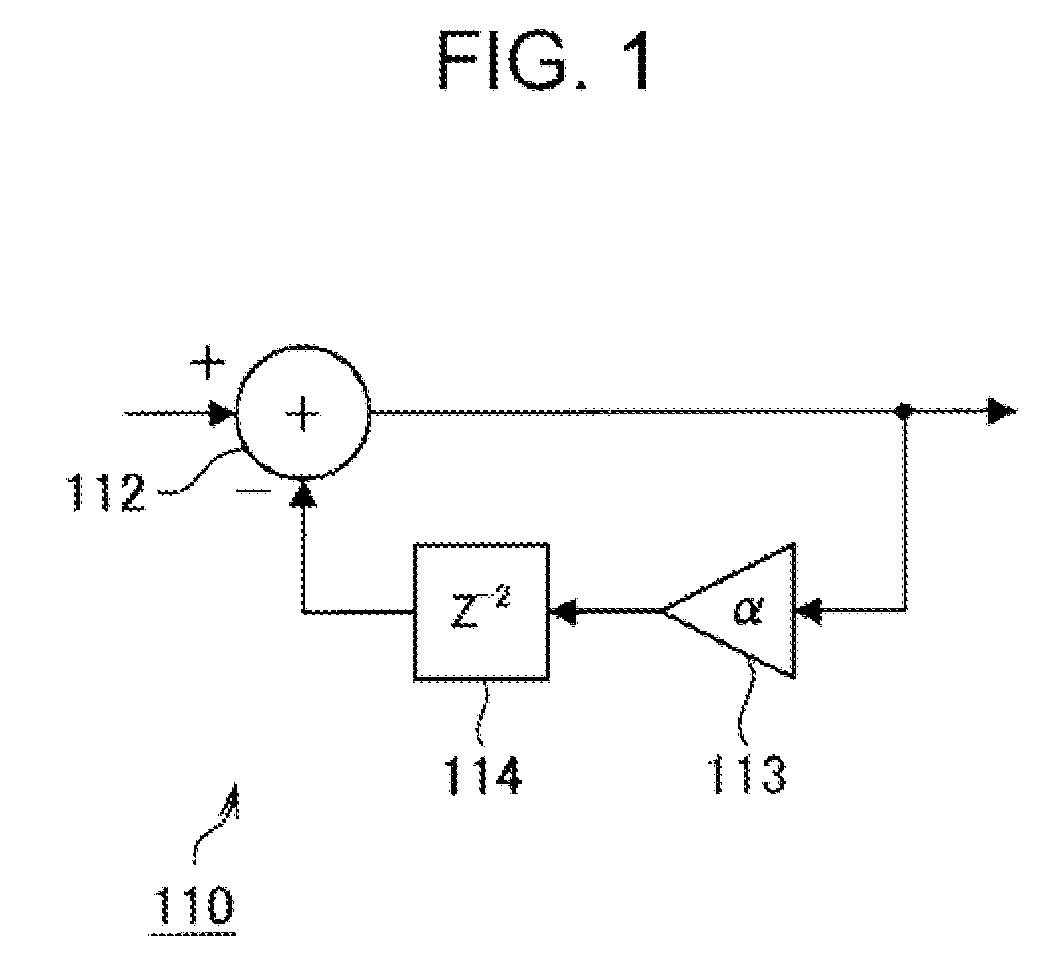
[0041]FIG. 1 is a diagram showing a configuration of a BPF according to the first embodiment of the present invention. As shown in FIG. 1, the BPF 110 according to the first embodiment of the present invention includes an adder 112, a multiplier 113, and a delay element 114.

[0042] The adder 112 subtracts a signal output from the delay element 114 from an input signal applied to the BPF 110, and the adder 112 outputs a resultant signal. The multiplier 113 multiplies the signal output from the adder 112 by a predetermined ...

second embodiment

[0085] In the first embodiment described above, the charge domain filter circuit capable of passing an input signal in the passband without producing degradation in high-frequency components is realized by making compensation in frequency characteristic in the passband so as to obtain the flat frequency characteristic up to the frequency of ¼t. In a second embodiment described below, compensation for frequency characteristic is made up to a frequency of ½t to realize a charge domain filter circuit having a flat frequency characteristic over a passband up to the frequency of ½t without producing degradation in high-frequency components.

[0086]FIG. 5 is a diagram showing a configuration of a BPF according to the second embodiment of the present invention. As shown in FIG. 5, the BPF 210 according to the second embodiment of the present invention includes an adder 212, a multiplier 213, and a delay element 214.

[0087] As with the adder 112 according to the first embodiment described ab...


PUM


Abstract

A charge domain filter device includes a SINC filter with a frequency characteristic expressed by a SINC function, and a bandpass filter connected to an output end of the SINC filter and having a frequency characteristic with a particular center frequency.

Description

CROSS REFERENCES TO RELATED APPLICATIONS [0001] The present invention contains subject matter related to Japanese Patent Application JP 2006-149367 filed in the Japanese Patent Office on May 30, 2006, the entire contents of which are incorporated herein by reference. BACKGROUND OF THE INVENTION [0002] 1. Field of the Invention [0003] The present invention relates to a filter device designed by charge domain operations (hereinafter, called a charge domain filter device). [0004] 2. Description of the Related Art [0005] In a wireless communication SoC (System On Chip) in which a RF (Radio Frequency) circuit and a digital circuit are integrated on a single chip using a CMOS (Complementary Metal Oxide Semiconductor) technique, it is known to accomplish filtering or decimation using current mode sampling at a high clock rate or an analog discrete-time signal processing technique such as a switched capacitor circuit whereby a small-sized low-power RF circuit is realized (see, for example, ...

Claims


Application Information

Patent Timeline
Patent Type & Authority Applications(United States)
IPC IPC(8): H03H7/03
CPCH03H19/004H03H15/00
Inventor IIDA, SACHIO
Owner SONY CORP
Why Eureka
Try Eureka