

Semiconductor device
a semiconductor device and read form technology, applied in the field of semiconductor devices, can solve the problems of difficult rewrite access (including write operation), difficult to guarantee data retention performance in the future, and worsening data characteristics
- Summary
- Abstract
- Description
- Claims
- Application Information
AI Technical Summary
Benefits of technology
Problems solved by technology
Method used
Image

Examples
Embodiment Construction
First Microcomputer
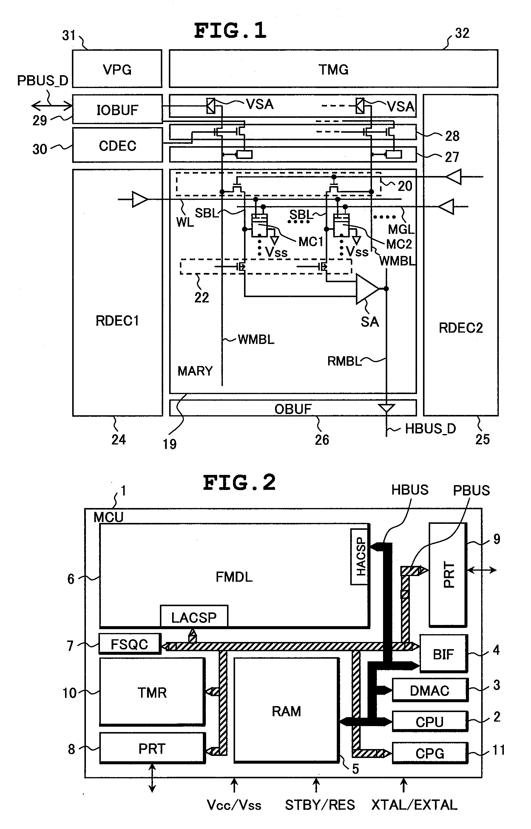
[0068]FIG. 2 shows a microcomputer (MCU) 1 according to an embodiment of the invention. The microcomputer 1 shown in the drawing is formed on a chip of semiconductor such as monocrystalline silicon, for example, by a complementary MOS IC manufacturing technique.
[0069]The microcomputer 1 is not particularly limited, but it has a two-bus structure having a high-speed bus HBUS and a peripheral bus PBUS. The high-speed bus HBUS and peripheral bus PBUS are not particularly limited, but they each include a data bus, an address bus and a control bus. Separation of buses into the two types of buses is intended to make the load to a bus smaller in comparison to the case where all the circuits are connected with a common bus in common, thereby to ensure a high-speed access operation.
[0070]To the high-speed bus HBUS are connected: a central processing unit (CPU) 2, which has an instruction control section and an execution section and executes an instruction; a direct memory ...
PUM
 Abstract
Description
Claims
Application Information