Conformal liner for gap-filling

a gap-filling and liner technology, applied in the field of semiconductor device manufacturing, can solve the problems of increasing the difficulty of completely filling gaps, forming undercut regions on the sidewall spacers of gate electrodes, and destroying silicon under the spacers, so as to improve reliability, improve manufacturing throughput, and improve reliability.

Inactive Publication Date: 2008-04-24
GLOBALFOUNDRIES INC +1
View PDF3 Cites 30 Cited by
  • Summary
  • Abstract
  • Description
  • Claims
  • Application Information

AI Technical Summary

Benefits of technology

[0006]An advantage of the present invention is a method of manufacturing semiconductor devices with improved reliability and high manufacturing throughput.
[0007]Another advantage of the present invention is a semiconductor device exhibiting improved reliability.
[0008]Additional advantages and other features of the present invention will be set forth in the description which follows and in part will be apparent to those having ordinary skill in the art upon examination of the following or may be learned from the practice of the present invention. The advantages of the present invention may be realized and obtained as particularly pointed out in the appended claims.
[0009]According to the present invention, the foregoing and other advantages are achieved in part by a method of manufacturing a semiconductor device, the method comprising: forming two gate electrode structures, spaced apart by a gap, on a semiconductor substrate; forming dielectric sidewall spacers, having undercut regions, on side surfaces of the gate electrode structures; depositing a conformal dielectric liner of (a) silicon oxide at a thickness of about 50 Å to about 500 Å; or (b) a material other than silicon oxide into the gap and into the undercut regions; and depositing a layer of dielectric material on the conformal dielectric liner and into the gap.
[0010]Certain embodiments of the present invention include depositing the conformal dielectric liner, the dielectric liner comprising a dielectric including, but not limited to (a) silicon oxide at a thickness of about 50 Å to about 500 Å; (b) silicon nitride; (c) silicon oxynitride; (d) silicon carbide; or (e) silicon oxycarbide. In yet other embodiments, the silicon oxide includes nitrogen and carbon content.
[0011]Embodiments of the present invention include forming sidewall spacers comprising an oxide liner, such as silicon oxide, extending along a side surface of the gate electrode stack and along an upper surface of the substrate, and a nitride layer, such as silicon nitride, on the oxide liner. Embodiments of the present invention further include depositing the dielectric liner by atomic layer deposition or pulsed layer deposition, at a thickness of about 50 Å to about 500 Å, such as at a thickness of about 10 to 100 atomic layers, e.g. about 50 atomic layers. After deposition of the conformal dielectric liner, the gap between the gate electrode stacks can be filled by one or more dielectric layers, as by depositing a layer of BPSG and annealing at a temperature of about 720° C. to about 840° C., or by depositing a layer of P-HDP oxide without annealing, particularly when the gate electrode structures comprise an upper layer of nickel silicide.

Problems solved by technology

As device dimensions shrink into the deep sub-micron regime, and the spacing between gate electrode structures decreases with increasing aspect ratio, such as at an aspect ratio of 3:1 or greater, it becomes increasingly more difficult to completely fill the gaps.
Exacerbating this problem, conventional fabrication techniques result in the formation of undercut regions on sidewall spacers of gate electrodes, typically proximate the upper layer of metal silicide and proximate the substrate.
Further, subsequent to silicidation, etching is conducted to remove unreacted metal remaining on the sidewall spacers, thereby attacking silicon under the spacers and exasperating the undercut regions.
The inability to adequately fill gaps between neighboring transistors, particularly the undercut regions in dielectric sidewall spacers, leads to void formation and open contacts with consequential shorting causing leakage and low production yields.
Such conventional gap-filling practices fall short of adequately addressing the void formation problem, particularly the problem of adequately filling undercut regions in dielectric sidewall spacers.
For example, P-HDP oxide does not exhibit sufficient fluidity to completely fill closely spaced apart high aspect ratio gaps, let alone the undercut regions in dielectric sidewall spacers.

Method used


Image

  • Conformal liner for gap-filling
  • Conformal liner for gap-filling
  • Conformal liner for gap-filling

Examples


Embodiment Construction

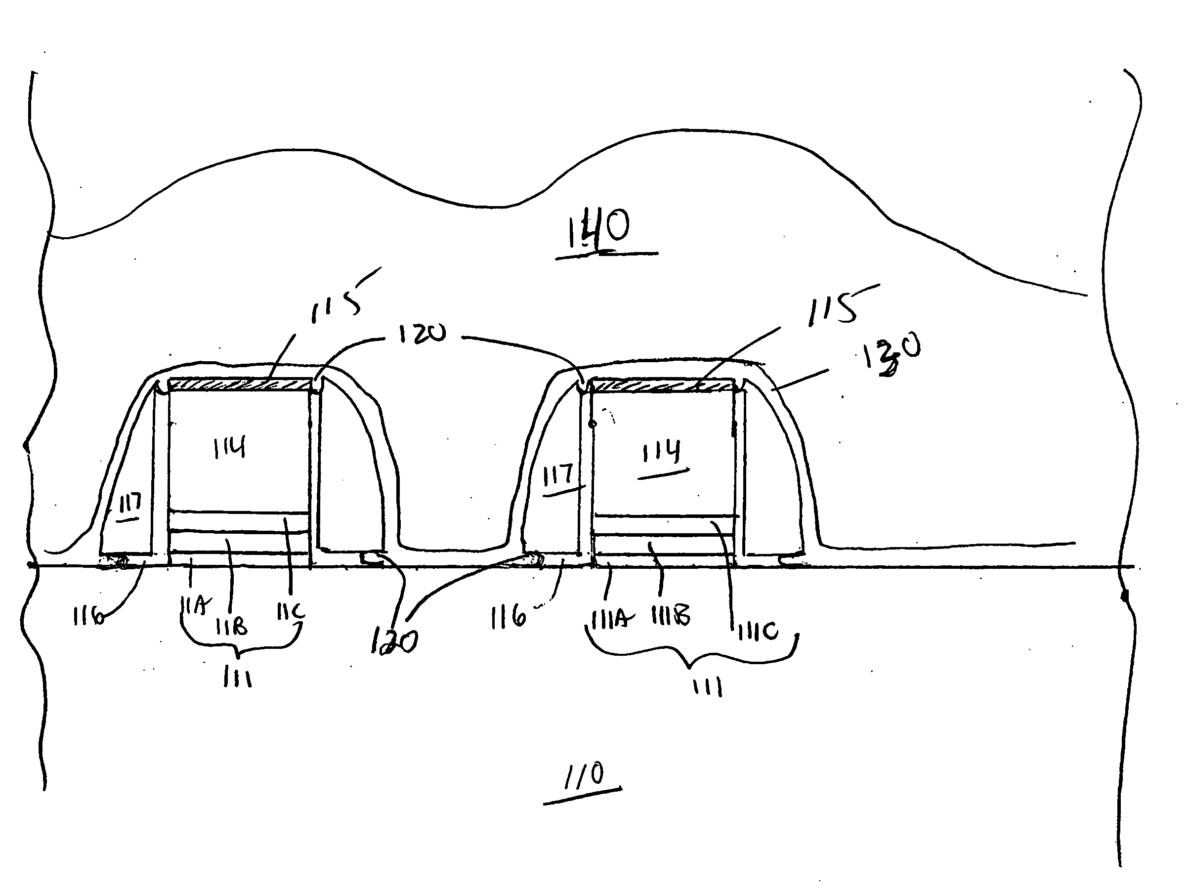
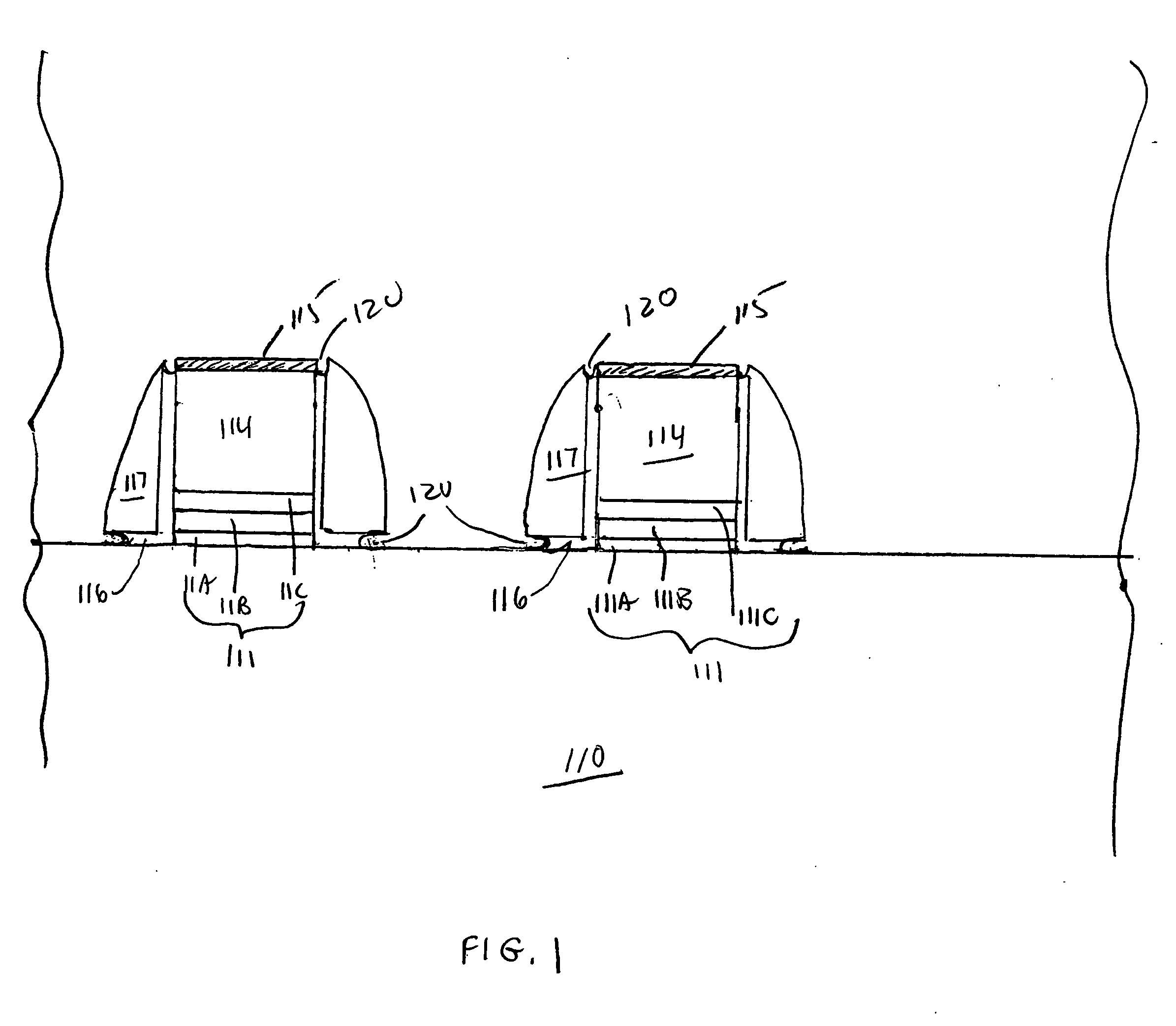
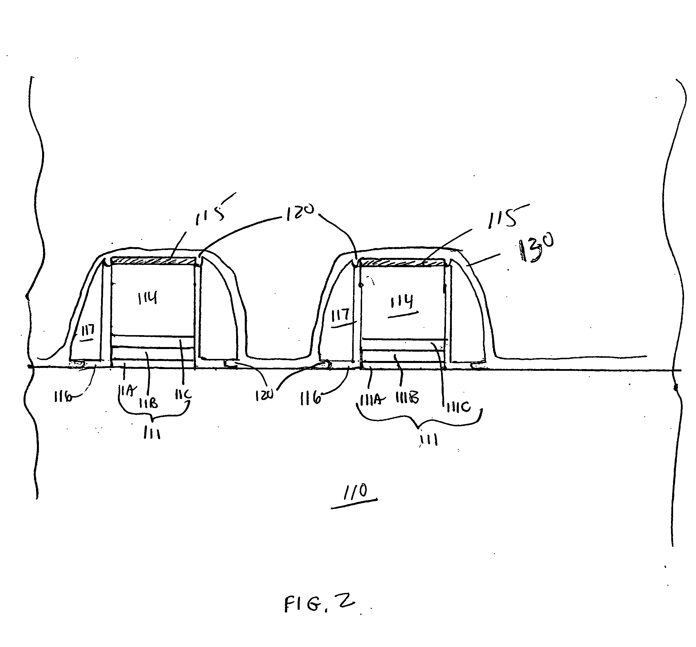
[0018]The present invention addresses and solves various reliability problems attendant upon conventional semiconductor fabrication techniques. These problems arise as semiconductor memory device dimensions continue to shrink, making it increasingly more difficult to deposit an ILD0 to effectively fill high aspect ratio gaps between closely spaced apart gate electrode structures, particularly wherein the gate electrode stacks comprise spacers with undercut regions. The inability to effectively fill such high aspect ratio gaps leads to various reliability problems and reduced yields.

[0019]The present invention addresses and solves that problem, and provides methodology enabling the fabrication of gate electrode structures with nickel silicide layers, by strategically depositing an extremely thin conformal layer of silicon oxide or silicon nitride as a liner in the gap and into the undercut portions. The silicon oxide liner can be deposited by various techniques, such as atomic layer ...


PUM


Abstract

Gap filling between features which are closely spaced is significantly improved by initially depositing a thin conformal layer followed by depositing a layer of gap filling dielectric material. Embodiments include depositing a thin conformal layer of silicon nitride or silicon oxide, as by atomic layer deposition or pulsed layer deposition, into the gap between adjacent gate electrode structures such that it flows into undercut regions of dielectric spacers on side surfaces of the gate electrode structures, and then depositing a layer of BPSG or P-HDP oxide on the thin conformal layer into the gap. Embodiments further include depositing the layers at a temperature less than 430° C., as by depositing a P-HDP oxide after depositing the conformal liner when the gate electrode structures include a layer of nickel silicide.

Description

FIELD OF THE INVENTION[0001]The present invention relates to a method of manufacturing semiconductor devices exhibiting high reliability, and to the resulting semiconductor devices. The present invention enjoys particular applicability in fabricating flash memory devices with improved data retention and improved gap filling.BACKGROUND OF THE INVENTION[0002]Semiconductor memory devices, such as erasable, programmable, read-only memories (EPROMs), electrically erasable programmable read-only memories (EEPROMs), and flash erasable programmable read-only memories (FEPROMs) are erasable and reusable, and are employed in various commercial electronic devices, such as computers, cellular telephones and digital cameras. There has recently evolved devices termed mirrorbit devices which do not contain a floating gate electrode. In mirrorbit devices, the gate electrode is spaced apart from the substrate by an oxide / nitride / oxide (ONO) stack, such as a silicon oxide / silicon nitride / silicon oxid...

Claims


Application Information

Patent Timeline
Patent Type & Authority Applications(United States)
IPC IPC(8): H01L21/76
CPCH01L21/76829H01L21/823468H01L21/823437H01L21/76837
Inventor WILSON, ERIKNGO, MINH-VANPHAM, HIEUHUERTAS, ROBERTYOU, LUTOKUNO, HIROKAZUNICKEL, ALEXANDERTRAN, MINH
Owner GLOBALFOUNDRIES INC
Why Eureka
Try Eureka