

Physical quantity sensor and method for manufacturing the same
a technology of physical quantity and sensor, which is applied in the direction of instruments, soldering apparatus, and semiconductor/solid-state device details, etc., can solve the problems of not being able to achieve the polyimide resin film is flexed, and the maintenance of a vacuum degree, so as to achieve the effect of reducing the thickness of the sensor
- Summary
- Abstract
- Description
- Claims
- Application Information
AI Technical Summary
Benefits of technology
Problems solved by technology
Method used
Image

Examples
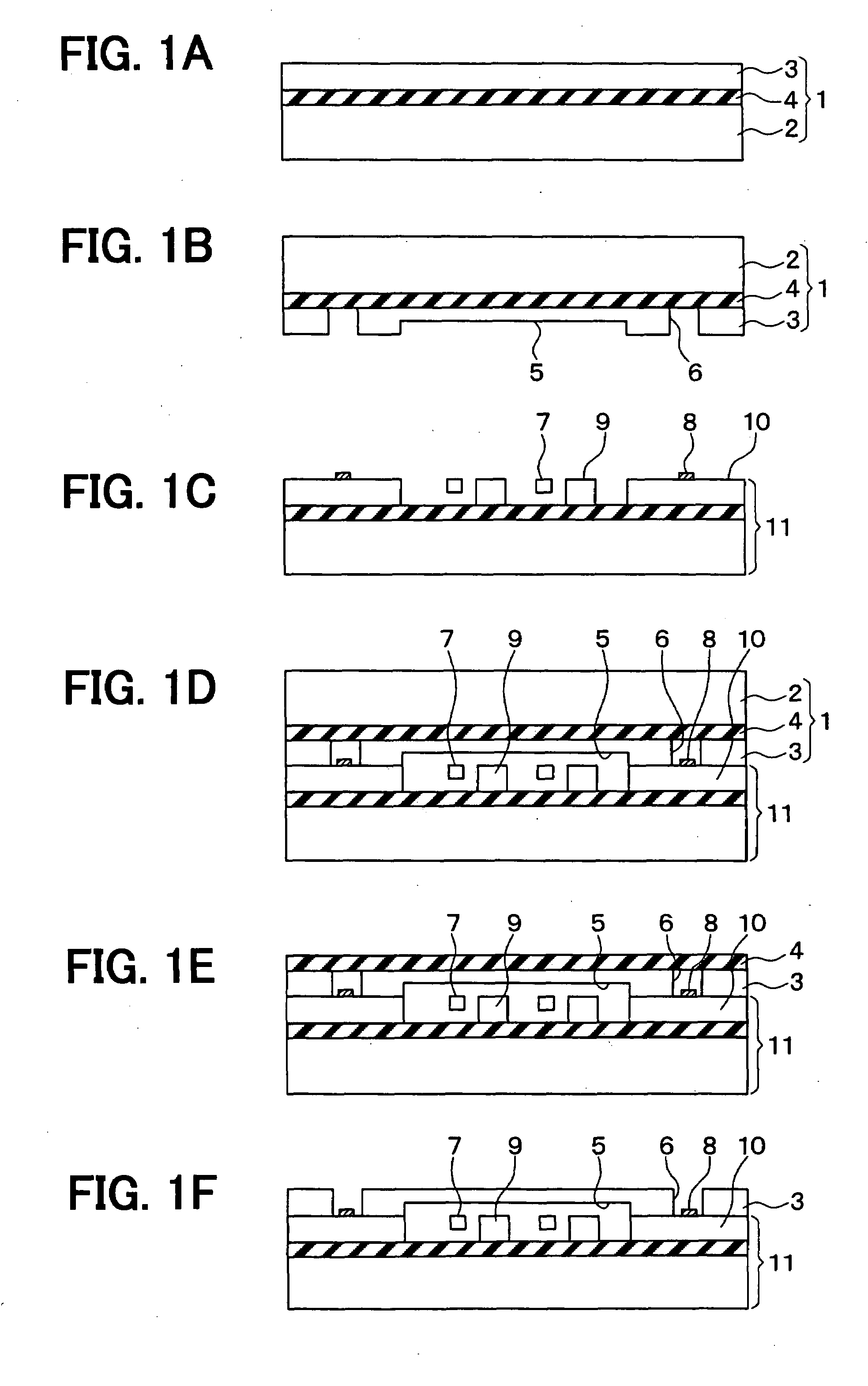
first embodiment
Modified Example of First Embodiment Mode
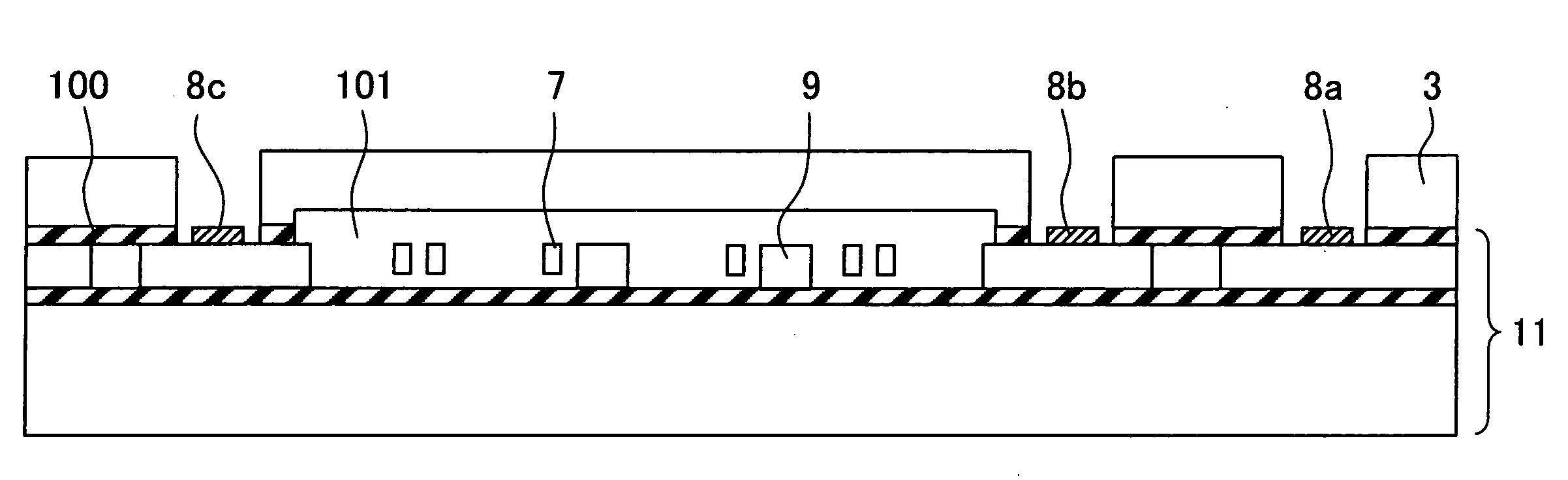
[0039]As mentioned above, in this embodiment mode, the SOI substrate 1 constructed by the single crystal silicon base 2, the burying oxide film 4 and the single crystal silicon layer 3 is used in a substrate for a cap for constructing the cap layer. However, this shows one mere example, and a substrate of another structure may be also used.
[0040]For example, as the substrate for a cap, a structure formed by replacing the single crystal silicon layer 3 with a polysilicon layer may be also used, and a structure formed by replacing the single crystal silicon layer 3 with a polysilicon base may be also used. Both the single crystal silicon layer 3 and the single crystal silicon base 2 may be also changed to a polysilicon layer and a polysilicon base. Further, no materials of the support base and the cap layer are limited to silicon, but e.g., alumina, SiC, etc. may be also used, and a metal such as Kovar, etc. may be also used. These materials ma...
second embodiment
Mode
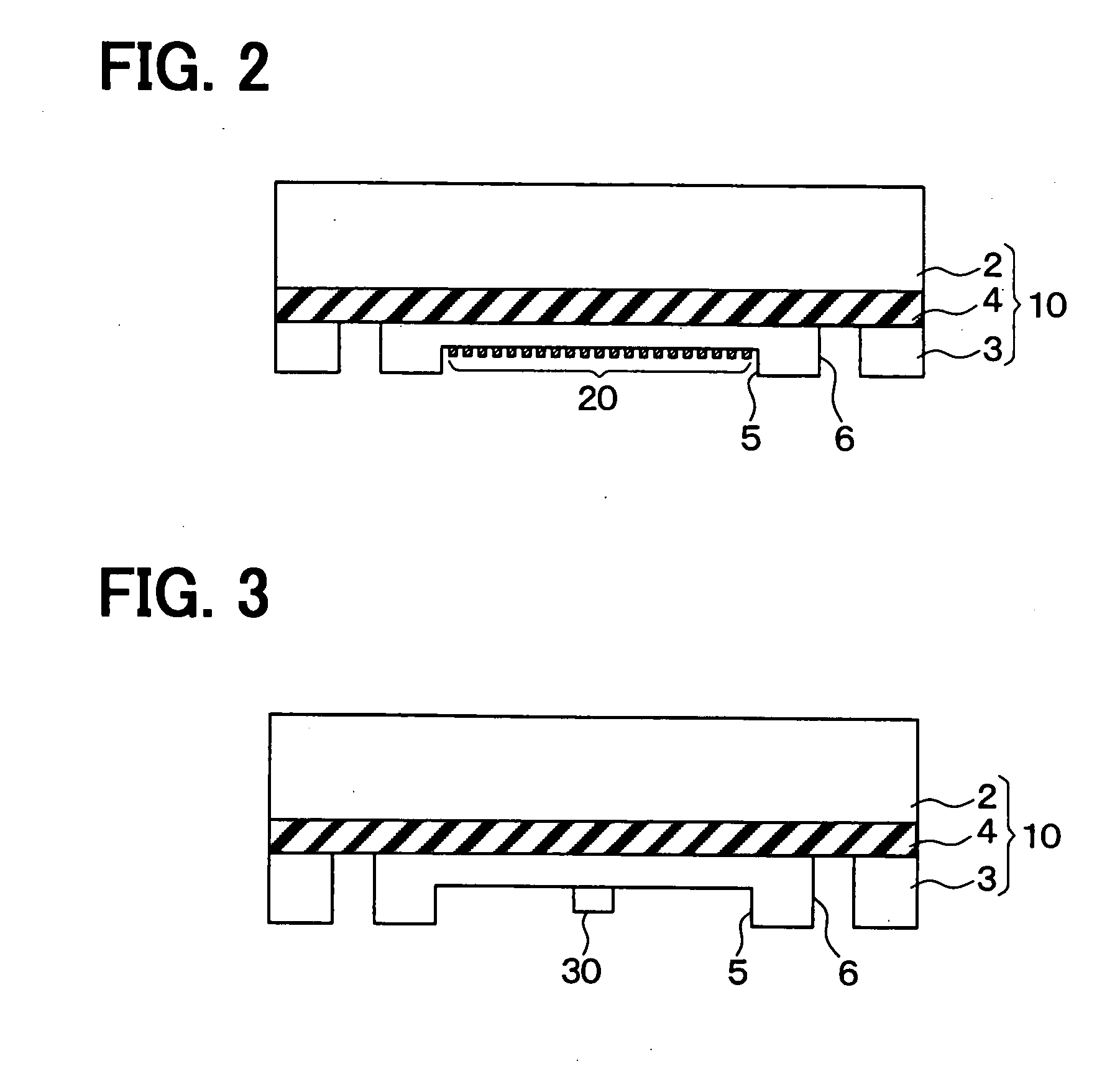
[0041]In a semiconductor dynamical amount sensor of this embodiment mode, the construction of the cap layer is changed with respect to the first embodiment mode. The others are similar to those of the first embodiment mode.
[0042]In this embodiment mode, as explained in the process shown in FIG. 1B of the first embodiment mode, a gettering layer is formed with respect to a structure in which the first concave portion 5 and the second concave portion 6 are formed in the single crystal silicon layer 3 of the SOI substrate 1. The others are similar to those of the first embodiment mode.
[0043]FIG. 2 is a cross-sectional view of the SOI substrate 1 in which the gettering layer 20 is formed after the process shown in the above FIG. 1B. As shown in this figure, the gettering layer 20 is formed on a bottom face of the first concave portion 5 in the single crystal silicon layer 3. This gettering layer 20 is arranged to more reliably maintain a high vacuum state when a spatial portion form...
third embodiment
Mode
[0045]In a semiconductor dynamical amount sensor of this embodiment mode, the construction of the cap layer is also changed with respect to the first embodiment mode. The others are similar to those of the first embodiment mode.
[0046]In this embodiment mode, as explained in the process shown in FIG. 1B of the first embodiment mode, a reinforcing rib portion is formed with respect to a structure in which the first concave portion 5 and the second concave portion 6 are formed in the single crystal silicon layer 3 of the SOI substrate 1. The others are similar to those of the first embodiment mode.
[0047]FIG. 3 is a cross-sectional view of the SOI substrate 1 forming the reinforcing rib portion therein. The reinforcing rib portion 30 reinforces the single crystal silicon layer 3 thinly formed by forming the first concave portion 5, and is partially arranged within the first concave portion 5. In this embodiment mode, the reinforcing rib portion 30 is constructed in a square shape in...
PUM
| Property | Measurement | Unit |
|---|---|---|
| temperature | aaaaa | aaaaa |
| thickness | aaaaa | aaaaa |
| thickness | aaaaa | aaaaa |
Abstract
Description
Claims
Application Information