Mirror Device, Mirror Array, Optical Switch, Mirror Device Manufacturing Method, and Mirror Substrate Manufacturing Method

a mirror array and mirror technology, applied in the direction of paper/cardboard containers, instruments, photomechanical equipment, etc., can solve problems such as spark discharge, achieve the effects of preventing movement, reducing the drift of the mirror, and high yield of non-defective units

Active Publication Date: 2008-05-01
NIPPON TELEGRAPH & TELEPHONE CORP
View PDF5 Cites 68 Cited by
  • Summary
  • Abstract
  • Description
  • Claims
  • Application Information

AI Technical Summary

Benefits of technology

[0020]An effect of the present invention is to suppress drift of the mirror. Since the antistatic structure is arranged in the space between the mirror and the lower substrate, the charge/discharge time constant to a part related to driving of the mirror can be small, or a part with a large charge/discharge time constant can be eliminated from the vicinity of the driving electrodes.
[0021]According to the present invention, since a metal layer is provided not only on one surface but also on the other surface of the mirror, warp of the mirror can be controlled.
[0022]According to the present invention, when the base, connectors, and mirror structure are formed on the buried insulating layer, a protective layer filling the spaces between them is formed. Even when the buried insulating layer in the mirror formation region is removed to expose...

Problems solved by technology

Frictional electricity causes spark discharge due to its high voltage.
However, the lar...

Method used


Image

  • Mirror Device, Mirror Array, Optical Switch, Mirror Device Manufacturing Method, and Mirror Substrate Manufacturing Method
  • Mirror Device, Mirror Array, Optical Switch, Mirror Device Manufacturing Method, and Mirror Substrate Manufacturing Method
  • Mirror Device, Mirror Array, Optical Switch, Mirror Device Manufacturing Method, and Mirror Substrate Manufacturing Method

Examples


first embodiment

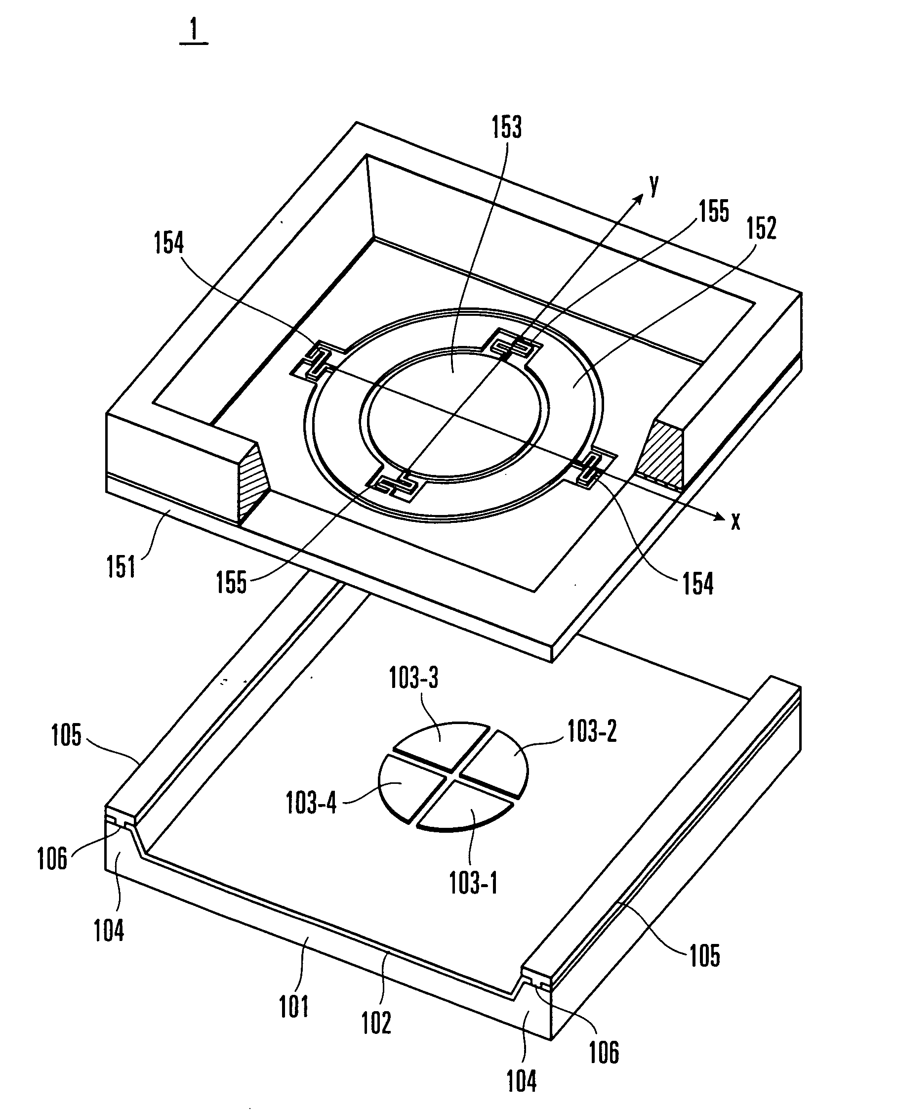
[0143]A mirror device 1 according to the first embodiment will be described below. As shown in FIGS. 1 and 2, an insulating layer 102 made of a silicon oxide film is formed on a lower substrate 101 of single-crystal silicon. Four driving electrodes 103-1 to 103-4 are provided on the insulating layer 102 at the center of the lower substrate 101. Supports 104 of single-crystal silicon are provided on both sides of the upper surface of the lower substrate 101.

[0144]In this embodiment, the insulating layer 102 on the surface of each support 104 is partially removed to form a contact hole 106. A metal layer 105 made of, e.g., Au is formed on the contact hole 106.

[0145]An upper substrate 151 has an annular gimbal 152 inside. A mirror 153 is provided inside the gimbal 152. For example, a Ti / Pt / Au layer (not shown) with a three-layered structure is formed on the upper surface of the mirror 153. Torsion springs 154 connect the upper substrate 151 to the gimbal 152 at two 180° opposite points...

second embodiment

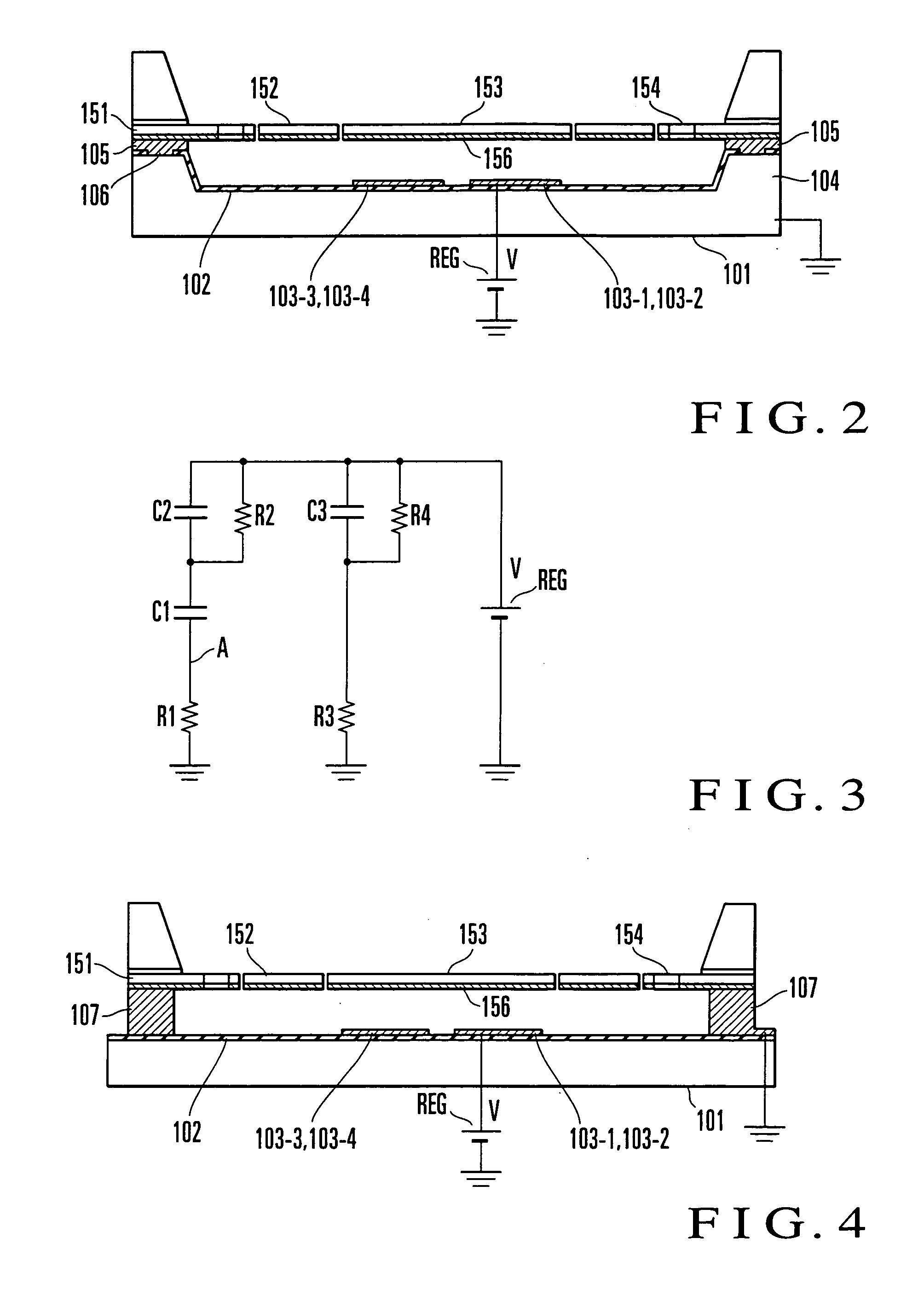
[0162]The second embodiment of the present invention will be described next with reference to FIG. 4. The same reference numerals as in FIGS. 1 and 2 denote the same parts in FIG. 4. In the first embodiment, the second potential is applied to the metal layer 156 through the lower substrate 101 and supports 104, which are made of single-crystal silicon. Instead, the second potential may be applied to a metal layer 156 through metal supports 107 formed on an insulating layer 102, as shown in FIG. 4. To form the supports 107, a metal such as Au is deposited by, e.g. plating. In the second embodiment, since it is possible to ensure electrical connection to the metal layer 156 without intervening a silicon layer, the potential of the lower surface of a mirror 153 can properly be set.

third embodiment

[0163]The third embodiment of the present invention will be described next with reference to FIG. 5. The same reference numerals as in FIGS. 1 and 2 denote the same parts in FIG. 5. In the first embodiment, the second potential is applied to the metal layer 156 through the lower substrate 101 and supports 104, which are made of single-crystal silicon. Instead, an insulating layer 102 on a lower substrate 101 may partially be removed to form contact holes 109, as shown in FIG. 5. Supports 108 made of, e.g., Au may be formed on the contact holes 109 to apply the second potential to a metal layer 156 through the supports 108. This facilitates electrical connection to the supports 108.

[0164]In the first to third embodiments, to obtain reliable electrical connection to the metal layer 156, an oxide film on the surface of the metal layer 105 or 156 or the supports 107 and 108 may be removed by, e.g., an acid. Not only mechanical contact but also solder such as an AuSn alloy or a conductiv...


PUM

PropertyMeasurementUnit
Angleaaaaaaaaaa
Temperatureaaaaaaaaaa
Thicknessaaaaaaaaaa

Abstract

A mirror device includes a mirror (153) which is supported to be pivotable with respect to a mirror substrate (151), a driving electrode (103-1-103-4) which is formed on an electrode substrate (101) facing the mirror substrate, and an antistatic structure (106) which is arranged in a space between the mirror and the electrode substrate. This structure can fix the potential of the lower surface of the mirror and suppress drift of the mirror by applying a second potential to the antistatic structure.

Description

TECHNICAL FIELD[0001]The present invention relates to an electrostatically driven mirror device having a mirror with changeable tilt angles, a mirror array having a plurality of mirror devices arranged two-dimensionally, an optical switch having the mirror array, a method of manufacturing the mirror device, and a method of manufacturing a mirror substrate included in the mirror device.BACKGROUND ART[0002]MEMS (Micro Electro Mechanical Systems) optical switches have received a great deal of attention as a hardware technology to implement large-scale optical switches. The most characteristic component of a MEMS optical switch is a MEMS mirror array. The MEMS mirror array includes a plurality of MEMS mirror devices (to be referred to as mirror devices hereinafter) arrayed two-dimensionally. A conventional mirror device (see, e.g., Japanese Patent No. 3579015) will be described below.[0003]As shown in FIGS. 107 and 108, an insulating layer 8002 made of a silicon oxide film is formed on ...

Claims


Application Information

Patent Timeline
IPC IPC(8): G02B26/08B05D5/06G03F7/20B29C65/00
CPCB81B3/004B81B3/0086B81B2201/045B81B2203/058Y10T29/49885G02B6/3556G02B6/3584G02B26/0841Y10T156/10G02B6/3518
Inventor SHIMOKAWA, FUSAOUCHIYAMA, SHINGOYAMAGUCHI, JOHJISATO, MAKOTOSASAKURA, KUNIHIKOMORITA, HIROFUMIINAGAKI, SHUICHIROMACHIDA, KATSUYUKIISHII, HIROMU
Owner NIPPON TELEGRAPH & TELEPHONE CORP
Why Eureka
Try Eureka