Method for Producing Direct Bonded Wafer and Direct Bonded Wafer

a technology of direct bonded wafer and direct bonded wafer, which is applied in the direction of semiconductor/solid-state device manufacturing, basic electric elements, electric apparatus, etc., can solve the problems of insufficient reduction of void count, inability to produce direct bonded wafer, and inability to reduce void generation in the junction plane, so as to achieve low void generation and low void count

Active Publication Date: 2008-05-01
SHIN-ETSU HANDOTAI CO LTD
View PDF2 Cites 230 Cited by
  • Summary
  • Abstract
  • Description
  • Claims
  • Application Information

AI Technical Summary

Benefits of technology

[0006]The present invention is accomplished in view of the aforementioned problems, and its object is to provide a method for producing a dire...

Problems solved by technology

Joining Si wafers together directly without sandwiching an insulator film such as an oxide film causes considerable generation of voids in the junction plane.
However, the method is a production method of the so-called SOI (Silicon On Insulator) wafers, and use of the method leaves a buried oxide film at the junction interface.
Consequently, a direct bonded wafer cannot be produced.
However, even use of this method cannot red...

Method used


Image

  • Method for Producing Direct Bonded Wafer and Direct Bonded Wafer
  • Method for Producing Direct Bonded Wafer and Direct Bonded Wafer
  • Method for Producing Direct Bonded Wafer and Direct Bonded Wafer

Examples


examples 1 to 6

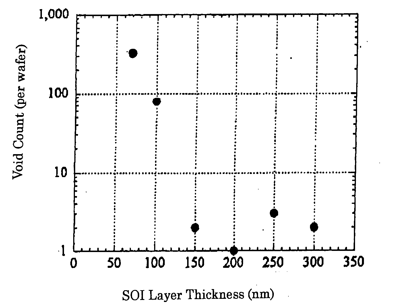
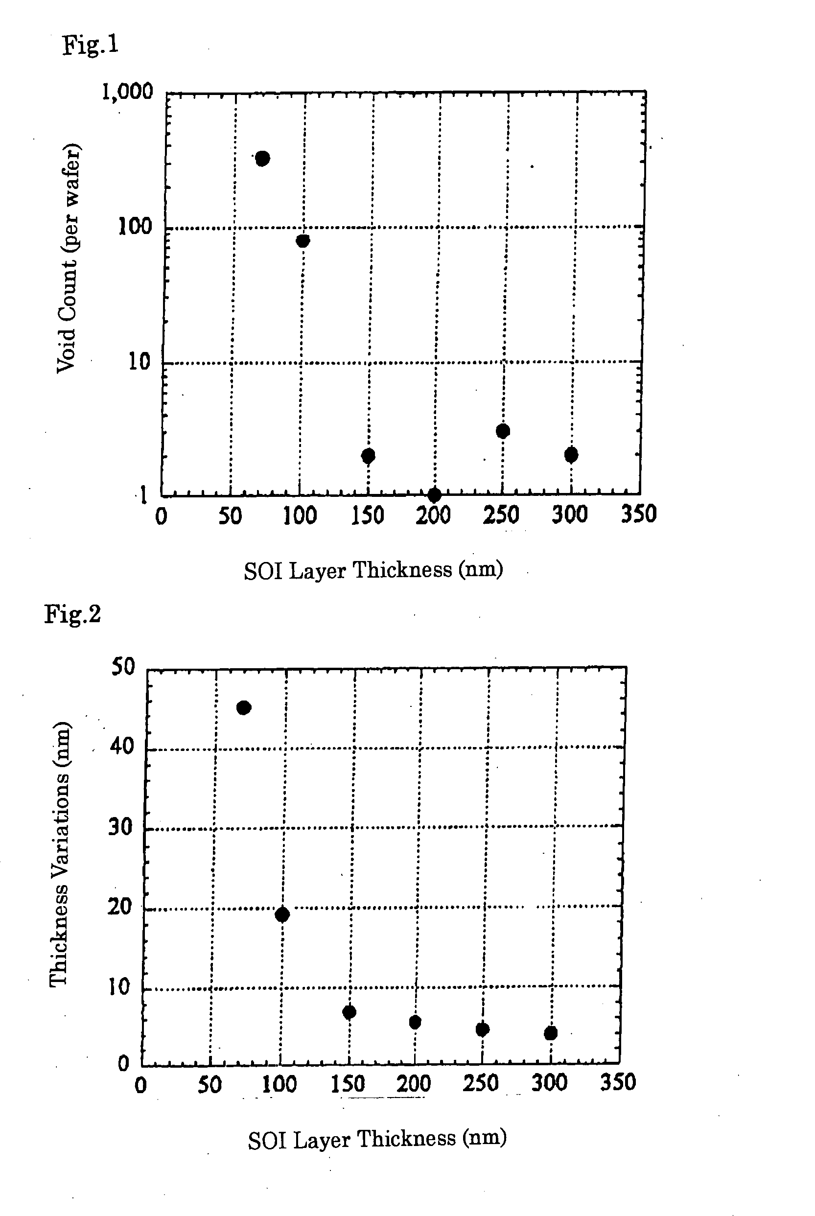
[0055]As a bond wafer, six Si wafers with a plane orientation of (110) and with a diameter of 12 inches (30.48 cm) were prepared. Each wafer underwent a heat treatment at 900 degrees C. for 5 minutes under a steam atmosphere to grow a 30 nm thick thermal oxide film on the surface of the bond wafer. Next, hydrogen ions were implanted to the respective bond wafers at an implantation depth of 400 nm. The bond wafers were superposed on six Si wafers with (100) which were prepared separately as base wafers via the thermal oxide film, respectively. The wafers underwent a heat treatment at 500 degrees C. for 30 minutes under nitrogen atmosphere to bond the wafers together, and also to separate the wafers at the hydrogen ion implanted layers. After that, a heat treatment at 1100 degrees C. for 1 hour under argon atmosphere was conducted to enhance bonding strength. At that moment, it was confirmed that generation of voids was reduced.

[0056]Then, the bond wafer sides of these wafers were thi...

examples 7 to 12

[0066]As a bond wafer, six Si wafers with a plane orientation of (110) and with a diameter of 12 inches (30.48 cm) were prepared. Each wafer underwent a heat treatment at 900 degrees C. for 5 minutes under a steam atmosphere to grow a 30 nm thick thermal oxide film on the surface of the bond wafer. Next, hydrogen ions were implanted to the respective bond wafers at an implantation depth of 400 nm. The bond wafers were superposed on six Si wafers with (100) which were prepared separately as base wafers via the thermal oxide film, respectively. The wafers underwent a heat treatment at 500 degrees C. for 30 minutes under nitrogen atmosphere to bond the wafers together, and also to separate the wafers at the hydrogen ion implanted layers. After that, a heat treatment at 1100 degrees C. for 1 hour under argon atmosphere was conducted to enhance bonding strength. At that moment, it was confirmed that generation of voids was reduced.

[0067]Then, the bond wafer sides of these wafers were thi...

example 13

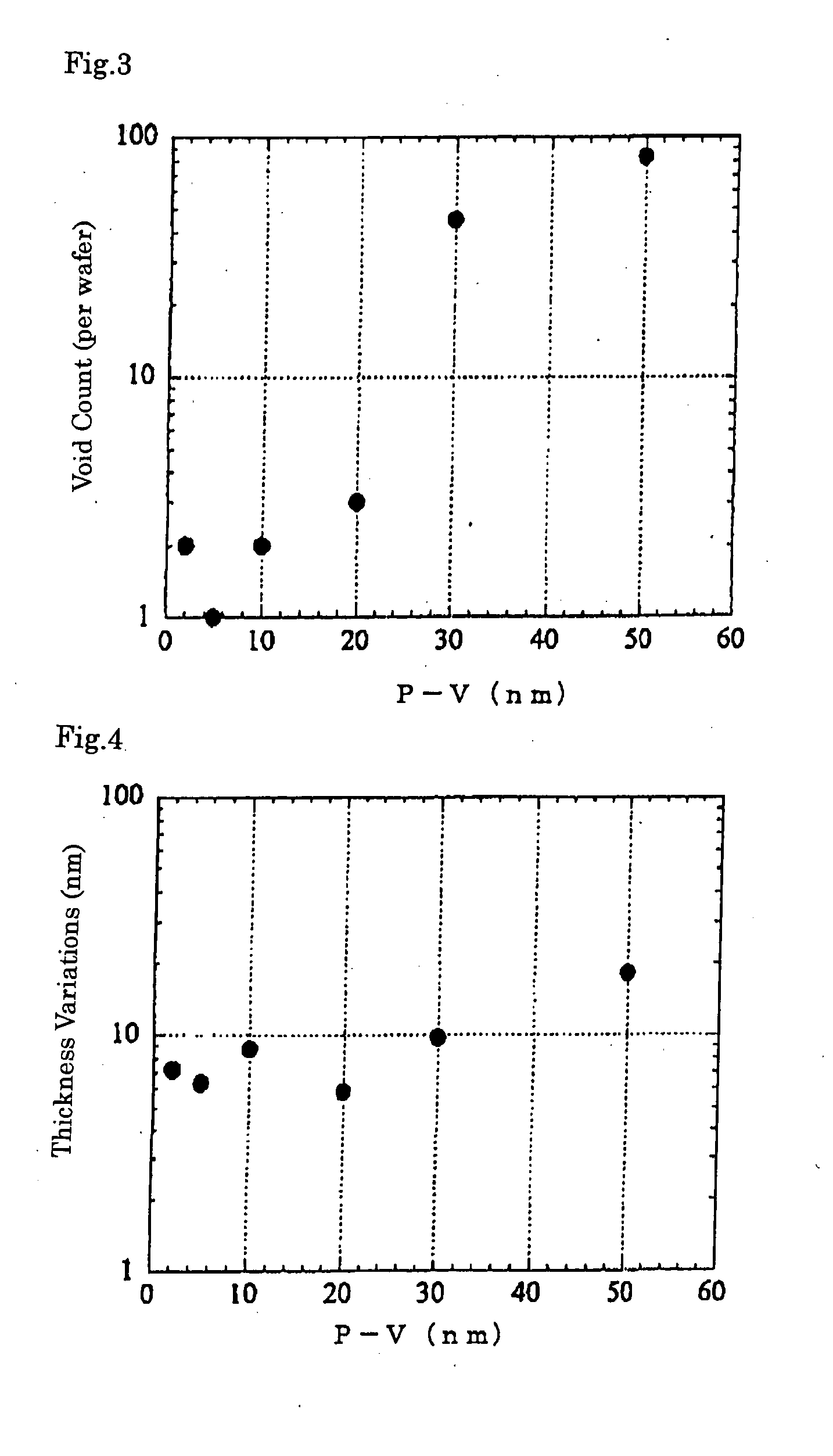
[0077]As a bond wafer, Si wafer with (110) and with a diameter of 12 inches (30.48 cm) was prepared. The wafer underwent a heat treatment at 900 degrees C. for 5 minutes under a steam atmosphere to grow a 30 nm thick thermal oxide film on the surface of the bond wafer. Next, hydrogen ions were implanted to the bond wafer at an implantation depth of 400 nm. The bond wafer was superposed on a (100) Si wafer which was prepared separately as base wafers via the thermal oxide film. The wafers underwent a heat treatment at 500 degrees C. for 30 minutes under nitrogen atmosphere to bond the wafers together, and also to separate the wafers at the hydrogen ion implanted layer. After that, a heat treatment at 1100 degrees C. for 1 hour under argon atmosphere was conducted to enhance bonding strength. At that moment, it was confirmed that generation of voids was reduced.

[0078]Then, the wafer was thinned by CMP polishing to have an SOI layer thickness of 250 nm before an annealing process. PV v...


PUM


Abstract

A method for producing a direct bonded wafer comprising: forming a thermal oxide film or a CVD oxide film on a surface of at least one of a bond wafer and a base wafer, and bonding the wafer to the other wafer via the oxide film; subsequently thinning the bond wafer to prepare a bonded wafer; and thereafter conducting a process of annealing the bonded wafer under an atmosphere including any one of an inert gas, hydrogen and a mixed gas of an inert gas and hydrogen so that the oxide film between the bond wafer and the base wafer is removed to bond the bond wafer directly to the base wafer. Thereby, there is provided a method for producing a direct bonded wafer in which generation of voids is reduced, and a direct bonded wafer with a low void count.

Description

TECHNICAL FIELD[0001]The present invention relates to a method for producing a direct bonded wafer and a direct bonded wafer which is obtained by bonding two wafers together directly and can be used for semiconductor devices.BACKGROUND ART[0002]Joining Si wafers together directly without sandwiching an insulator film such as an oxide film causes considerable generation of voids in the junction plane. There is a fact that bonding wafers together either or both of which is oxidized and has an oxide film with a certain thickness or more can produce less voids than the case of bonding wafers directly. However, the method is a production method of the so-called SOI (Silicon On Insulator) wafers, and use of the method leaves a buried oxide film at the junction interface. Consequently, a direct bonded wafer cannot be produced.[0003]On the other hand, a method for producing a direct bonded wafer is disclosed in Japanese Unexamined Patent Application Publication No. 2000-36445. In the method...

Claims


Application Information

Patent Timeline
IPC IPC(8): H01L21/46
CPCH01L21/76254H01L21/2007
Inventor KOBAYASHI, NORIHIROISHIZUKA, TORUOHTA, TOMOHIKOAGA, HIROJINAGAOKA, YASUO
Owner SHIN-ETSU HANDOTAI CO LTD
Why Eureka
Try Eureka