Semiconductor devices and fabrication process thereof

a technology of semiconductor devices and fabrication processes, applied in the direction of semiconductor devices, transistors, electrical devices, etc., can solve the problems of gate electrodes having a higher interfacial energy level, introducing nitrogen into gate insulating films, and reducing the deposition rate, so as to increase the film-forming time, prevent any damage, and increase resistance

Inactive Publication Date: 2008-05-08
SONY CORP
View PDF3 Cites 29 Cited by
  • Summary
  • Abstract
  • Description
  • Claims
  • Application Information

AI Technical Summary

Benefits of technology

[0017]In one embodiment of the present invention, there is thus provided a semiconductor device having an insulated gate transistor provided with a semiconductor substrate and a gate electrode arranged on the semiconductor substrate via a gate insulating film, wherein the gate electrode includes: an electrically-conductive buffer film for preventing any damage which would occur if a main gate electrode portion were formed directly over the gate insulating film, and the main gate electrode portion formed over the buffer film.
[0018]In the semiconductor device according to the present invention, the buffer film is arranged between the gate insulating film and the main gate electrode portion. Even when the main gate electrode portion has been formed by a plasma-assisted film-forming process, the gate insulating film has, therefore, been protected from any adverse effect of the plasma, for example, the adverse effect of nitrogen introduction. As the main gate electrode portion, it is accordingly possible to use one formed by a plasma-assisted film-forming process. On the other hand, the buffer film is arranged to avoid any adverse effect of the plasma and therefore, is not demanded to be formed thick. The formation of the buffer film, therefore, brings about neither an adverse effect which would otherwise be produced by an increase in resistance nor an adverse effect of an increased film-forming time. A film formed by a thermal film-forming process can be used as the buffer film.
[0019]In another embodiment of the present invention, there is also provided a process for the fabrication of a semiconductor having an insulated gate transistor provided with a semiconductor substrate and a gate electrode arranged on the semiconductor substrate via a gate insulating film, the process including the step of forming the gate electrode, wherein the gate-electrode-forming step includes the following steps of: forming an electrically-conductive buffer film for preventing any damage which would occur if a main gate electrode portion were formed directly over the gate insulating film, and forming the main gate electrode portion over the buffer film.
[0020]In the fabrication process according to the present i...

Problems solved by technology

When a metal gate electrode is formed by a thermal film-forming process, for example, thermal CVD, problems arise in that the resulting gate electrode is provided with a higher resistance and moreover, the deposition rate becomes lower.
However, any attempt to form a gate insulating film with a nitrogen-containi...

Method used


Image

  • Semiconductor devices and fabrication process thereof
  • Semiconductor devices and fabrication process thereof
  • Semiconductor devices and fabrication process thereof

Examples


first embodiment

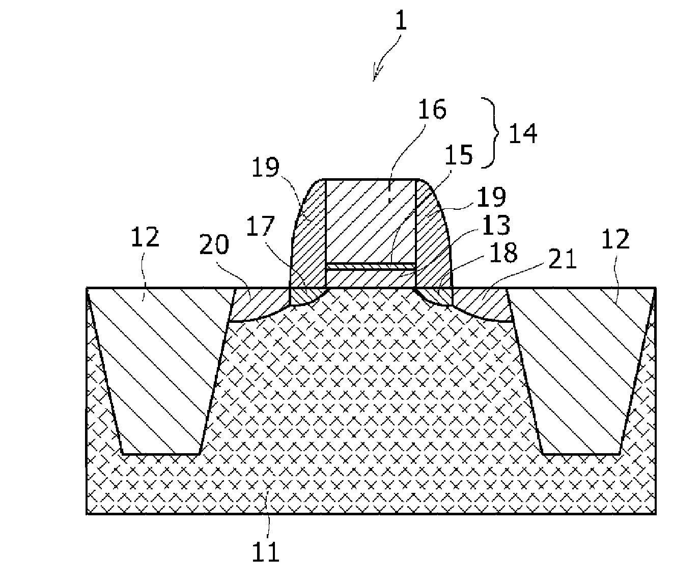
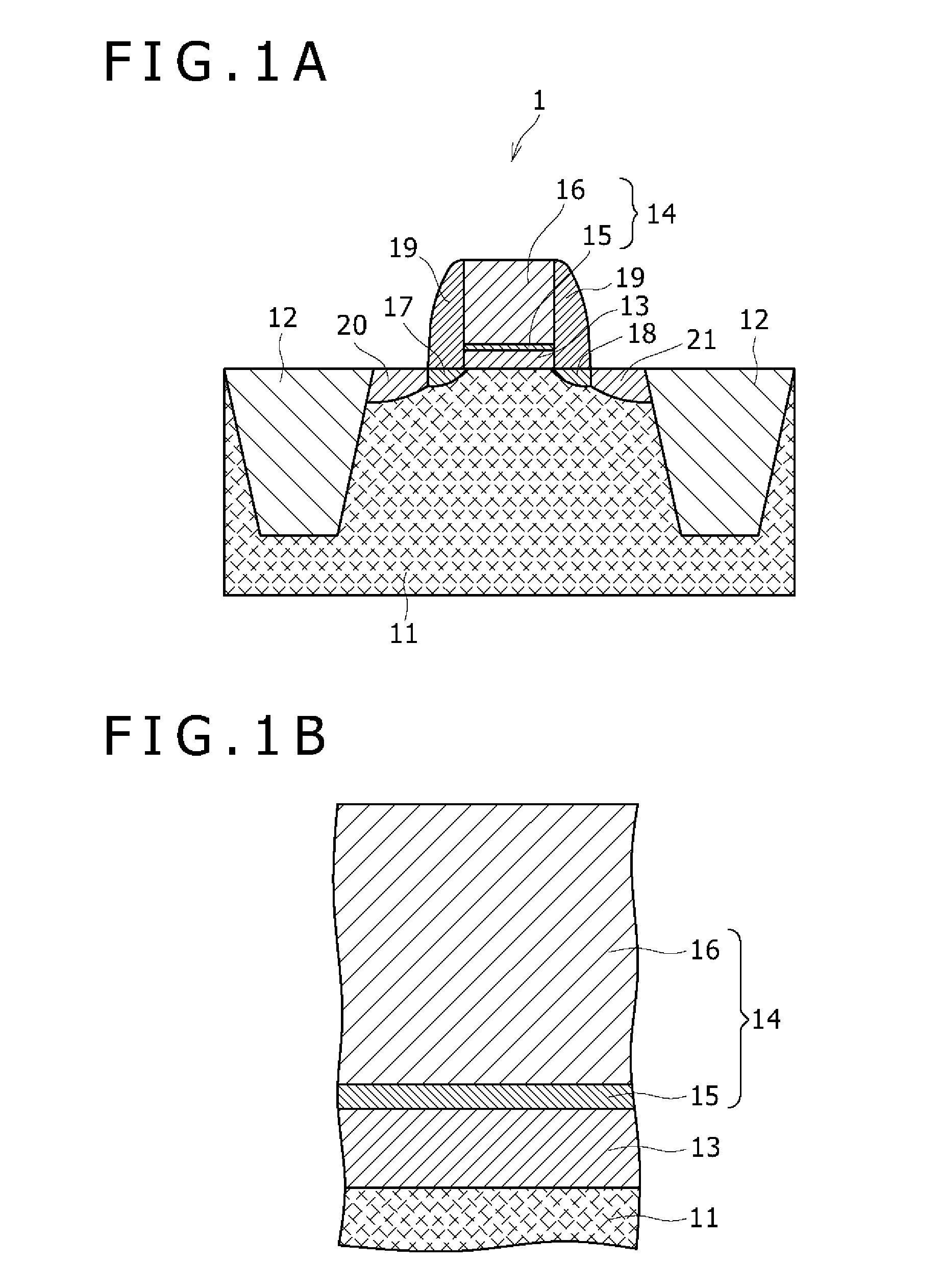
[0032]Referring first to FIGS. 1A and 1B, a description will hereinafter be made of an insulated gate field-effect transistor as a semiconductor according to the present invention.

[0033]As illustrated in FIGS. 1A and 1B, a semiconductor device 1 is constructed as will be described below. In a semiconductor substrate 11, insulating regions 12 are formed for the isolation of the resulting device. The semiconductor substrate 11 is formed of a silicon substrate, for example. A gate electrode 14 is formed over the semiconductor substrate 11 with a gate insulating film 13 interposed therebetween. This gate electrode 14 is composed of an electrically-conductive buffer film 15 and a main gate electrode portion 16. Upon formation of the gate electrode 14 as an upper layer, the buffer film 15 serves to prevent any damage to the associated lower layer. For example, the gate insulating film 13 is formed of a silicon oxide (SiO2) film. As an alternative, the gate insulating film 13 may be formed...

second embodiment

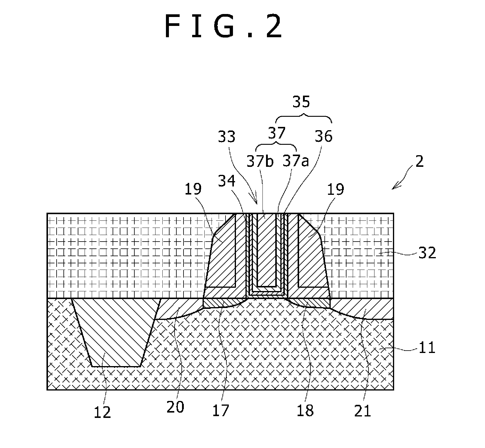
[0040]With reference to FIG. 2, a semiconductor device 2 according to the present invention, which includes a MOSFET with a buried gate structure, will be described next.

[0041]As depicted in FIG. 2, an insulating region 12 is formed in a semiconductor substrate 11 to isolate the resulting device. The semiconductor substrate 11 is formed of a silicon substrate, for example. A gate electrode forming trench 33 in which a gate electrode is to be formed is formed over the semiconductor substrate 11. This gate electrode forming trench 33 was formed by forming a dummy electrode (not shown), forming an interlayer insulating film 32, and then removing the dummy electrode.

[0042]Extension regions 17, 18 are formed in the semiconductor substrate 11 on opposite sides of the gate electrode forming trench 33. In addition, sidewall spacers 19 are formed on sidewalls of the gate electrode forming trench 33. Further, source and drain regions 20, 21 are formed in the semiconductor substrate 11 such th...

third embodiment

[0048]Referring next to FIGS. 3A through 3F, a fabrication process according to the present invention will be described.

[0049]As illustrated in FIG. 3A, gate insulating regions 12 are formed in a semiconductor substrate 11 to isolate the device. As the semiconductor substrate 11, a silicon substrate is used for example. The semiconductor substrate 11 with the insulating regions 12 formed therein is next cleaned at a surface thereof. In this cleaning, the substrate surface is decontaminated with a mixed solution of ammonia, hydrogen peroxide solution and pure water. Subsequently, the substrate 11 with the insulating regions 12 formed therein is dipped for 60 seconds in an aqueous solution of hydrofluoric acid (HF / H2O: 1 / 100) to remove a natural oxide film.

[0050]As shown in FIG. 3B, a gate insulating film 13 is next formed over the semiconductor substrate 11. As an example of this gate insulating film 13, a thermally grown oxide film (SiO2 film) can be formed by thermally oxidizing th...


PUM


Abstract

A semiconductor device has an insulated gate transistor provided with a semiconductor substrate and a gate electrode arranged on the semiconductor substrate via a gate insulating film. The gate electrode includes an electrically-conductive buffer film for preventing any damage, which would occur if a main gate electrode portion were formed directly over the gate insulating film, and the main gate electrode portion formed over the buffer film. A fabrication process for the semiconductor device is also disclosed.

Description

CROSS REFERENCES TO RELATED APPLICATIONS[0001]The present invention contains subject matter related to Japanese Patent Application JP 2006-067269 filed in the Japanese Patent Office on Mar. 13, 2006, the entire contents of which being incorporated herein by reference.BACKGROUND OF THE INVENTION[0002]1. Field of the Invention[0003]This invention relates to semiconductor devices making use of metal gate electrodes, and also to a process for the fabrication of the same.[0004]2. Description of the Related Art[0005]High integration and high-speed operation of MOS transistors have been progressively materialized by their miniaturization on the basis of the scaling laws, and a gate length as short as 0.1 μm is now about to be achieved. Keeping in step with this, thinner gate insulating films have been increasingly adopted. In a transistor with a gate length of 0.1 μm or smaller, for example, it is necessary to reduce the thickness of a gate insulating film to 2 nm or less. This miniaturiza...

Claims


Application Information

Patent Timeline
IPC IPC(8): H01L21/336H01L29/78
CPCH01L21/28088H01L21/823842H01L29/4966H01L29/7833H01L29/6656H01L29/6659H01L29/66545
Inventor HIRANO, TOMOYUKITAI, KAORI
Owner SONY CORP
Why Eureka
Try Eureka