Semiconductor device, wiring of semiconductor device, and method of forming wiring

a semiconductor device and semiconductor technology, applied in the direction of semiconductor devices, semiconductor/solid-state device details, electrical equipment, etc., can solve the problems of increasing the manufacturing step and cost accordingly, the wiring resistance of the wiring becomes large, and the layer cracking and breakage of the semiconductor element cannot always be prevented

Inactive Publication Date: 2008-05-08
DENSO CORP
View PDF13 Cites 30 Cited by
  • Summary
  • Abstract
  • Description
  • Claims
  • Application Information

AI Technical Summary

Benefits of technology

[0013] In view of the above-described problem, it is an object of the present invention to provide a semiconductor device, in which a bonding impact force is suitably absorbed to prevent a crack in a lower layer and a break in a semiconductor element located below a bonding portion of the semiconductor device.

Problems solved by technology

It has been confirmed that the crack in the layers and the break in the semiconductor element cannot always be prevented.
In particular, it is likely that the wiring resistance of the wiring become large, because the wiring become very thin at the lowest layer.
As a result, manufacturing step and cost are increased accordingly.
The vibration may cause cracks in the interlayer dielectric film.
As a result, the aluminum film is thinned and cannot suitably reduce the bonding impact force.

Method used


Image

  • Semiconductor device, wiring of semiconductor device, and method of forming wiring
  • Semiconductor device, wiring of semiconductor device, and method of forming wiring
  • Semiconductor device, wiring of semiconductor device, and method of forming wiring

Examples


first embodiment

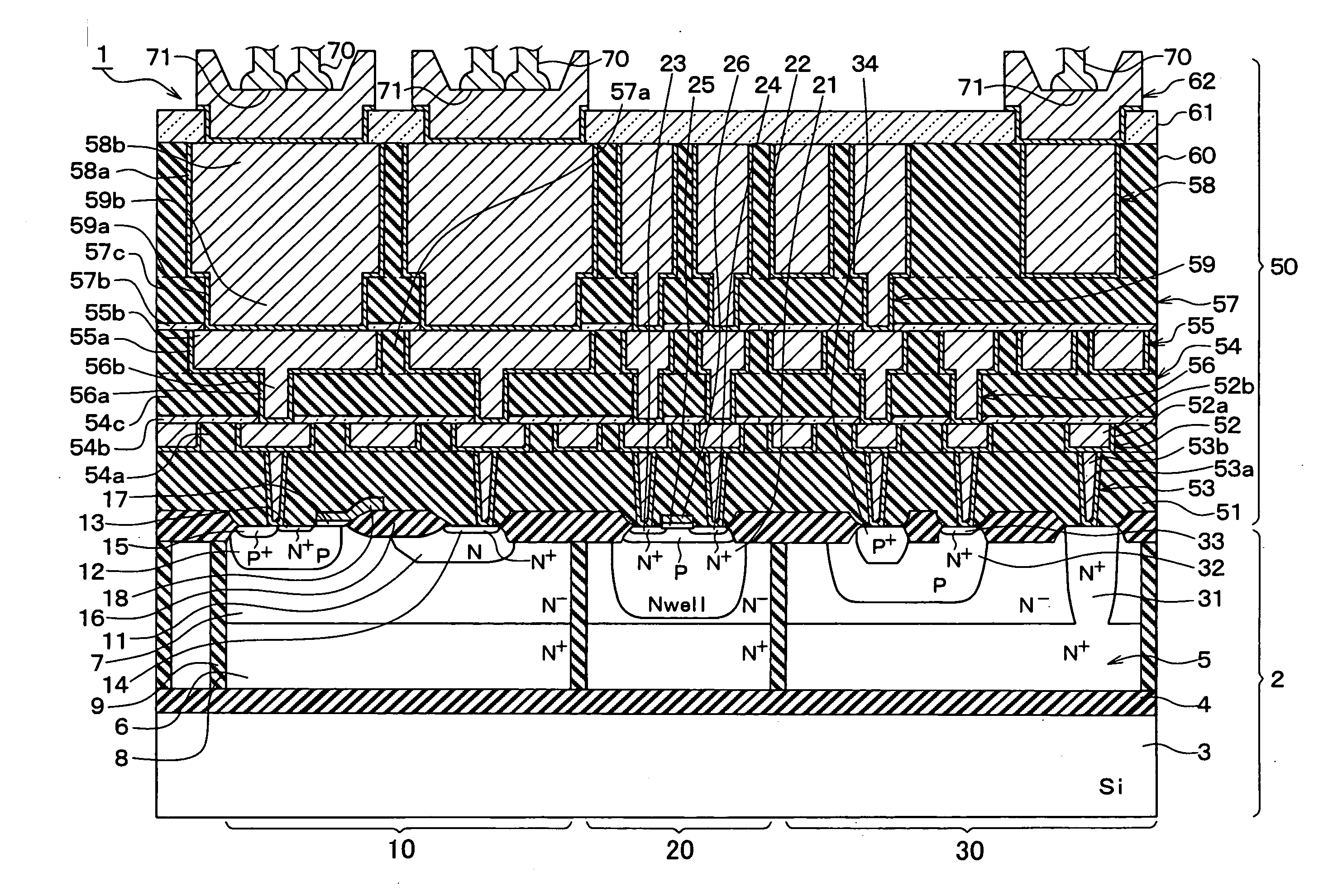
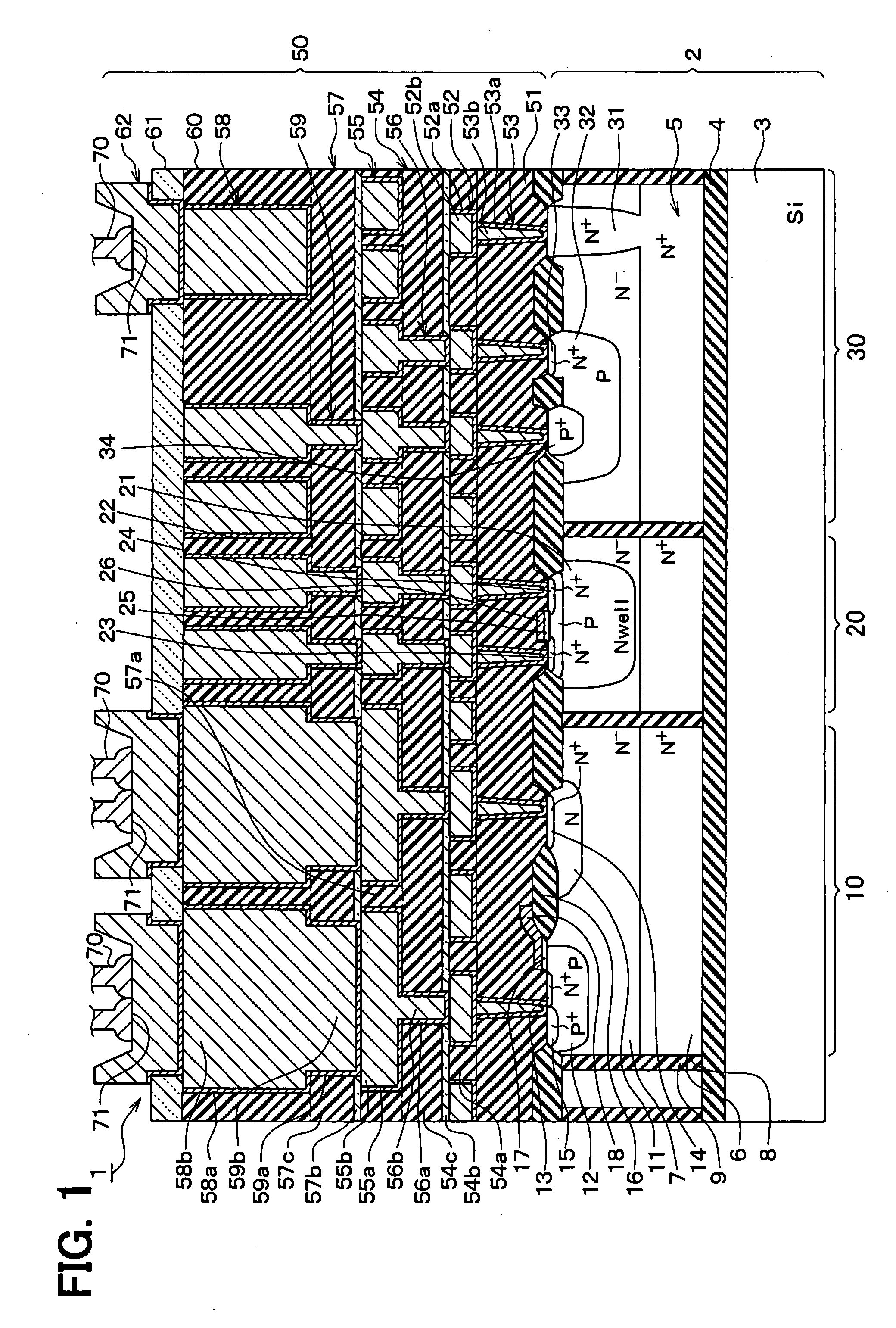
[0040] Referring to FIG. 1, a semiconductor device 1 according to a first embodiment of the present invention includes a laterally diffused metal oxide semiconductor (LDMOS) 10, a complementary metal-oxide-semiconductor (CMOS) 20, and a bipolar transistor 30, which are integrated together to form an integrated circuit. The semiconductor device 1 is formed by using a silicon on insulator (SOI) substrate 2.

[0041] The SOI substrate 2 has a structure such that a silicon layer 5 as an active layer is disposed on a surface of a silicon substrate 3 through an insulator layer 4. The silicon substrate 3 acts as a supporting substrate, and the insulator layer 4 is a silicon oxide film, for example. The silicon layer 5 includes a N+ type layer 6 and a N− type 7 formed to a surface portion of the N+ type layer 6. The LDMOS 10, the CMOS 20, and the bipolar transistor 30 are formed in first, second, and third regions of the silicon layer 5. The first, second, and third regions are separated from...

second embodiment

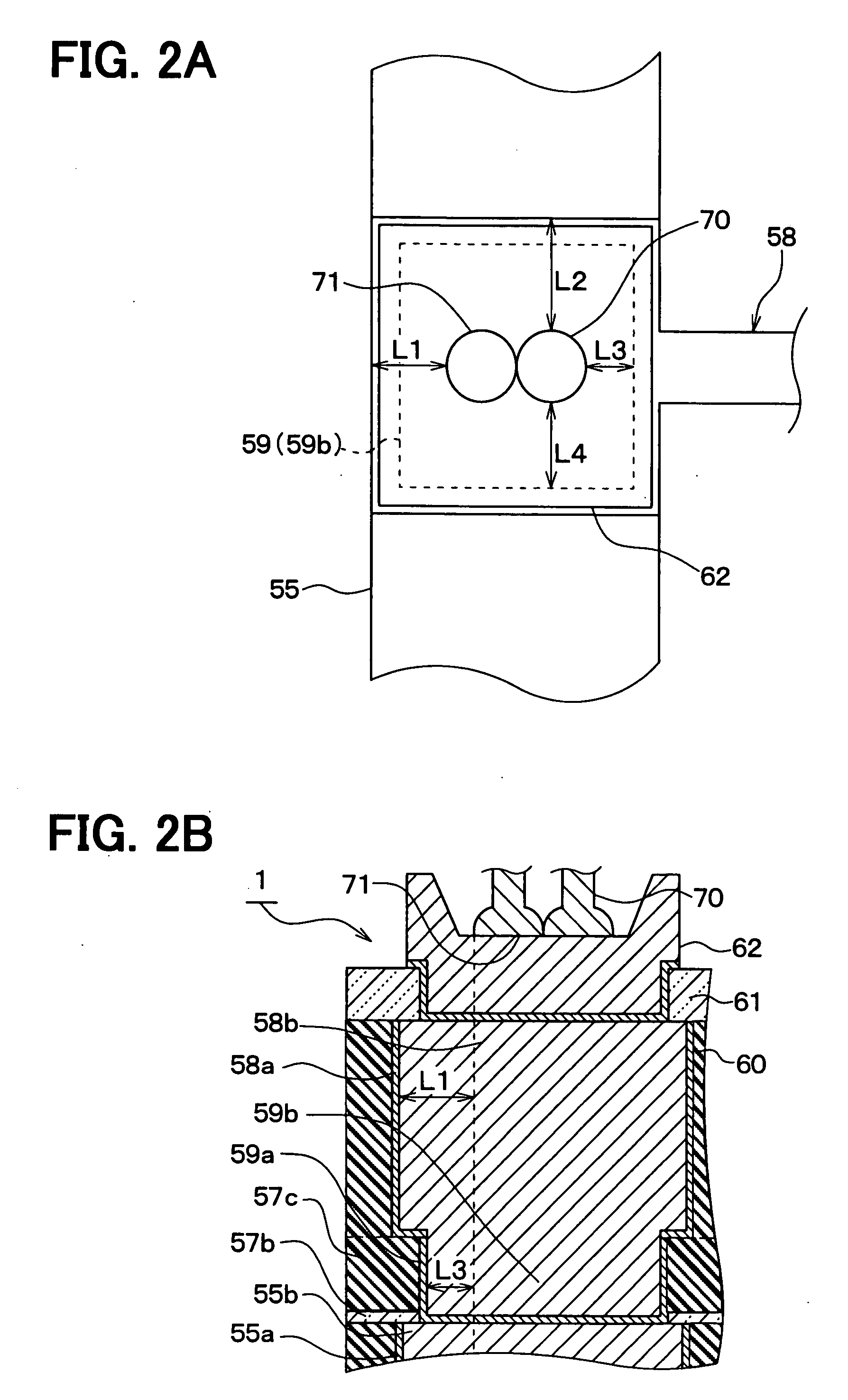
[0098] A second embodiment of the second embodiment is described below with reference to FIG. 13. As shown in FIG. 13, the second embodiment refers to a case where free space 90 exists on a layer where the top wiring-electrode layer 58 is formed. The free space 90 is a region other than regions in which the LDMOS 10, a logic circuit constructed with the CMOS 20 and the bipolar transistor 30, and the bonding pad 62 for electrically connecting each portion of the logic circuit are formed.

[0099] A dummy pattern 91 of the top wiring-electrode layer 58 is formed to the free space 90, and a bonding pad 62 is formed on the dummy pattern 91 so that a bonding wire 70 is connectable to the top wiring-electrode layer 58 through the bonding pad 62. As long as the number of pins of a package accommodating the semiconductor device 1 is allowed, the pins and the dummy pattern 91 are connected through the bonding wire 70.

[0100] According to the second embodiment, the dummy pattern 91 of the top w...

third embodiment

[0110] A third embodiment of the present invention is described below with reference to FIGS. 16A-18. The third embodiment refers to a method of forming a wiring layer having a large thickness. For example, the wiring forming method according to the third embodiment can be applied to form the top wiring-electrode layer 58 of the semiconductor device 1.

[0111] (First Interlayer Dielectric Film Forming Process)

[0112] First, a substrate 110 is prepared. As shown in FIG. 16A, a lower wiring layer 111 is formed on a surface 110a of the substrate 110 in advance. The substrate 110 is a silicon substrate, a SOI substrate, or the like. The lower wiring layer 111 is formed with copper (Cu), aluminum (Al), molybdenum (Mo), or the like. The lower wiring layer 111 may be provided with a barrier layer (not shown) for diffusion prevention.

[0113] Then, a first interlayer dielectric film 112 is formed on the surface 110a of the substrate 110. The first interlayer dielectric film 112 has a first th...


PUM


Abstract

A semiconductor device includes a substrate, an element formed in the substrate, an insulation film formed on the substrate, wiring layers, and an electrode pad. The wiring layers are multilayered and electrically coupled to the element through the insulation film. The electrode pad is electrically coupled to a top wiring layer of the wiring layers. The top wiring layer is configured to be a top wiring-electrode layer that doubles as an electrode layer disposed under the electrode pad. The electrode layer of the top wiring-electrode layer is disposed directly above the element. The electrode pad and the electrode layer are multilayered to form a pad structure.

Description

CROSS CHECK TO RELATED APPLICATION [0001] This application is based on and incorporates herein by reference Japanese Patent Applications No. 2006-288711 filed on Oct. 24, 2006, No. 2006-288715 filed on Oct. 24, 2006, No. 2006-289982 filed on Oct. 25, 2006, and No. 2007-150431 filed on Jun. 6, 2007. FIELD OF THE INVENTION [0002] The present invention relates to a semiconductor device, wiring of the semiconductor device, and a method of forming the wiring. BACKGROUND OF THE INVENTION [0003] Wire bonding techniques have been proposed that allow wire bonding on an electrode pad of a semiconductor device in a case where a semiconductor element is formed below the electrode pad. In U.S. Pat. No. 6,261,939 corresponding to JP-A-2003-518739, thicknesses of an interlayer dielectric layer and a wiring layer positioned below the electrode pad is increased to between 1 micrometer (μm) and 2 μm. In JP-A-H8-236706, a wiring layer is multilayered below the electrode pad. Thus, a crack in the layer...

Claims


Application Information

Patent Timeline
Patent Type & Authority Applications(United States)
IPC IPC(8): H01L23/52H01L21/4763
CPCH01L2924/1305H01L2924/0002H01L21/76838H01L23/5283H01L23/53238H01L24/03H01L24/05H01L24/45H01L24/48H01L24/49H01L2224/04042H01L2224/05006H01L2224/05082H01L2224/05147H01L2224/05166H01L2224/05181H01L2224/05187H01L2224/05572H01L2224/05611H01L2224/05616H01L2224/05624H01L2224/05639H01L2224/05644H01L2224/45015H01L2224/45144H01L2224/48463H01L2224/48611H01L2224/48616H01L2224/48624H01L2224/48639H01L2224/48644H01L2224/49111H01L2224/85205H01L2924/01005H01L2924/01013H01L2924/01014H01L2924/01015H01L2924/01022H01L2924/01025H01L2924/01028H01L2924/01029H01L2924/0103H01L2924/01042H01L2924/01046H01L2924/01047H01L2924/0105H01L2924/01073H01L2924/01074H01L2924/01078H01L2924/01079H01L2924/01082H01L2924/04941H01L2924/04953H01L2924/05042H01L2924/13091H01L2924/14H01L2924/19043H01L2924/20753H01L2924/30107H01L2924/01006H01L2924/01019H01L2924/01024H01L2924/01033H01L2924/01068H01L2224/02166H01L2224/05554H01L2924/00014H01L2924/00H01L2224/05552H01L2924/01204H01L2924/013H01L2924/00013
Inventor KUZUHARA, TAKESHIKOMURA, ATSUSHIKATADA, MITSUTAKANARUSE, TAKAYOSHI
Owner DENSO CORP
Why Eureka
Try Eureka