
Eureka
For R&D, Eureka makes reading and utilizing patents & technical documents easy.
Eureka AIR
Designed for self-driven R&D workflows. Generate viable solutions, solve complex R&D challenges, empower your innovation with AI.

Eureka Materials
Designed for material experts only. Revolutionize your material R&D, from search, analyze, to developing new materials.

TechResearch
Generate reliable direction feasibility study reports for your R&D in just a few steps.

TechSeek
Discover and master advanced knowledge NOW. Basics, ideas, possibilities, all at once.

TechMind
As an expert in R&D Theories, TechMind can generates customized viable solutions instantly.

TechRisk
Analyze your overall solution with one click, know your potential R&D risks in advance.

TechMonitor
Get weekly tech updates, stay abreast of the latest tech innovations and key insights.
Digital Wireless Receiver
- Summary
- Abstract
- Description
- Claims
- Application Information
AI Technical Summary
Benefits of technology
Problems solved by technology
Method used
Image

Examples
first embodiment
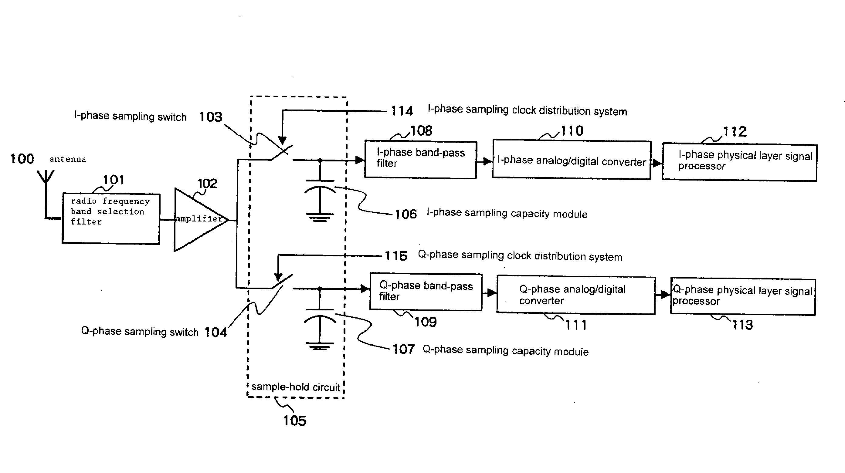
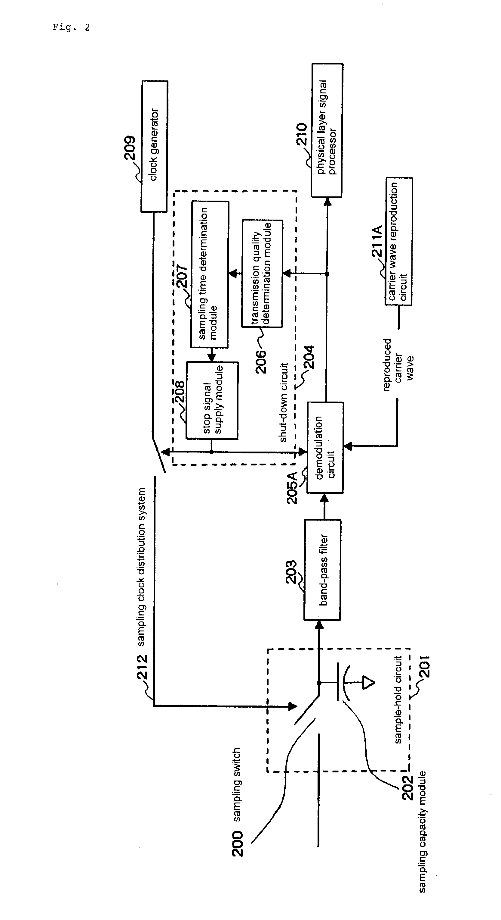
[0070]FIG. 2 is a block diagram of the digital wireless receiver according to a first embodiment of the present invention. Clock generator 209 generates sampling clocks. Carrier wave reproduction circuit 211A reproduces the carrier wave. Sample-hold circuit 201 receives sampling clocks that are supplied from clock generator 209 by way of sampling clock distribution system 212, samples the input signal (the output signal of amplifier 102 in FIG. 1), and then holds for a predetermined period of time to produce a discrete time signal. Band-pass filter 203 eliminates unnecessary aliasing components and undesired frequency components that have been generated by discretization of the signal. Demodulation circuit 205A compares the input signal from band-pass filter 203 and the reproduced carrier wave in an extremely short period of time to produce a baseband signal and transmits the baseband signal to physical layer signal processor 210. Shut-down circuit 204 receives the baseband signal t...
second embodiment
[0085]FIG. 5 is a block diagram of the digital wireless receiver of the second embodiment of the present invention. The present embodiment differs from the digital wireless receiver of the first embodiment in that the carrier wave reproduced in carrier wave reproduction circuit 211B is applied as a sampling clock to demodulation circuit 205B and timing synchronization is established when reading the modulated waveform.
[0086]Operation of the present embodiment will be explained below. Here, only the operation that differs from the previously described first embodiment is presented.
[0087]After the input signal has undergone frequency conversion from Fin to Fc, the input signal is applied as input to demodulation circuit 205B. FIG. 6 shows the operation of demodulation circuit 205B. As shown in FIG. 6, during 1 / Fr in which modulation is carried out at one symbol, demodulation circuit 505B is activated in synchronization with the rise time Ta of the reproduced carrier wave and is operat...
third embodiment
[0091]FIG. 7 is a block diagram of the digital wireless receiver of a third embodiment according to the present invention. The present embodiment differs from the digital wireless receiver of the first embodiment in that carrier waves of four phases in which the phase is delayed every 90° are reproduced in carrier wave reproduction circuit 211C, and these carrier waves of four phases are all applied as input to demodulation circuit 205C.
[0092]Operation of the digital wireless receiver of the present embodiment will now be explained below. Here, only operations that differ from the previously described first embodiment are presented.
[0093]The frequency of the modulated signal input is converted from Fin to Fc and then applied as input to demodulation circuit 205C. At the same time, reproduced carrier waves in which the phase has been delayed 0°, 90°, 180°, and 270°, respectively, from the carrier wave are also applied as input to demodulation circuit 205C. FIG. 8 shows the operation ...
PUM
 Abstract
Description
Claims
Application Information
 - R&D Engineer
- R&D Manager
- IP Professional
- Industry Leading Data Capabilities
- Powerful AI technology
- Patent DNA Extraction
Browse by: Latest US Patents, China's latest patents, Technical Efficacy Thesaurus, Application Domain, Technology Topic, Popular Technical Reports.
© 2024 PatSnap. All rights reserved.Legal|Privacy policy|Modern Slavery Act Transparency Statement|Sitemap|About US| Contact US: help@patsnap.com