

Selective electroless deposition for solar cells
- Summary
- Abstract
- Description
- Claims
- Application Information
AI Technical Summary
Benefits of technology
Problems solved by technology
Method used
Image

Examples
first embodiment
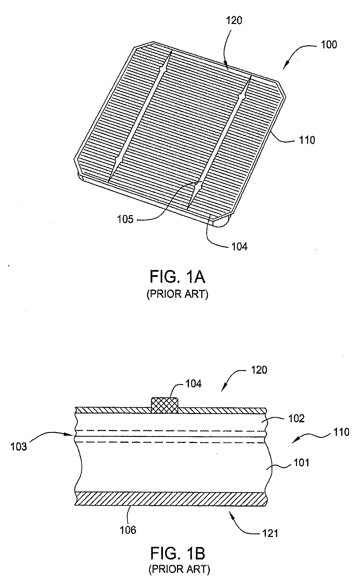
[0042]FIG. 3A illustrates a partial schematic cross section of a solar cell according to the invention. The portion of the solar cell shown in FIG. 3A is a contact structure 300. Contact structure 300 is similar to that of PUM cell 130 described above in conjunction with FIG. 1B and identical numbers are used to depict common elements. Contact structure 300 is formed on a wafer 110 that consists of a material suitable for use as a substrate in a solar cell, such as silicon (Si), germanium (Ge), and gallium arsenide (GaAs), among others. Contact structure 300 includes a p-type base region 101, an n-type emitter region 102, and a p-n junction region 103 disposed therebetween. In other examples of solar cells, the n-type region and the p-type region may be transposed, i.e., the p-type region may serve as the emitter and the n-type region may serve as the base. For clarity, however, solar cells following the standard convention of a p-type base region and an n-type emitter region are us...
second embodiment
[0047]FIG. 3B illustrates a partial schematic cross section of a solar cell according to the invention. The portion of the solar cell shown in FIG. 3B is a contact structure 370. Contact structure 370 includes two through-holes 131 through wafer 110. One through-hole 131 is in a p-type base region 101, another through-hole 131 is in an n-type emitter region 102, and a p-n junction region 103 is disposed therebetween. A contact 334A fills the through-hole 131 in p-type base region 101 and a contact 334B fills the through-hole 131 in n-type emitter region 102. In addition, contacts 334A, 334B may not be disposed on light-receiving surface 132, thereby eliminating any shadowing effect on light-receiving surface 132. Contacts 334A, 334B are otherwise similar in make-up to the various configurations of contact 334 described above in conjunction with FIG. 3A. In this aspect, a solar cell may include a plurality of contacts that each form an ohmic contact with an equal number of respective...
third embodiment
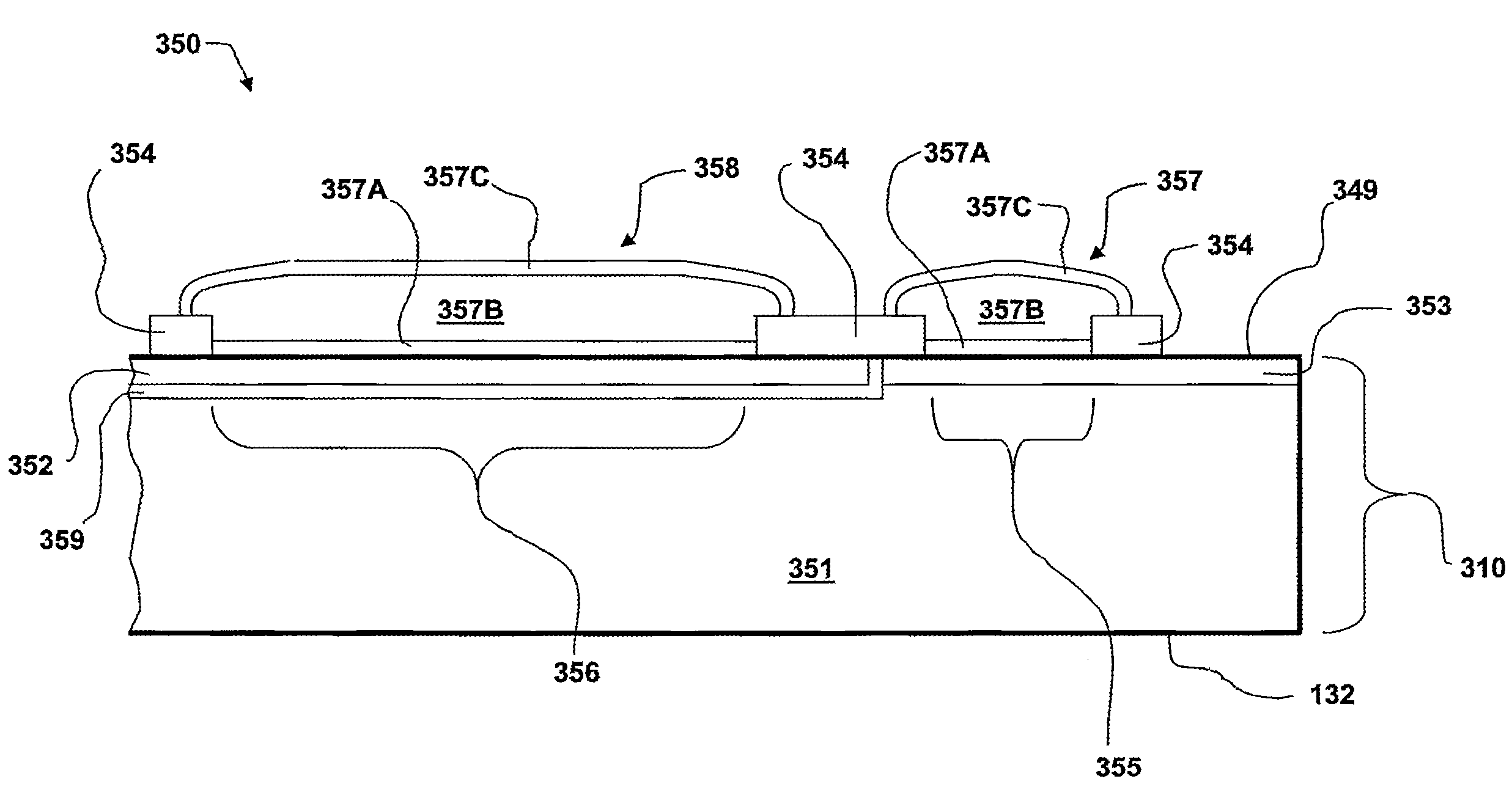
[0049]FIG. 3C illustrates a partial schematic cross section of a solar cell according to the invention. The portion of the solar cell shown in FIG. 3C is a backside contact structure 350. In this embodiment, the light-receiving surface 132 of a solar cell substrate 310 (shown at the bottom) may be contact-free, i.e. there is no shadowing of the substrate's light-receiving surface by contacts disposed on the frontside of the substrate. All contacts and metallization buses are made on the backside surface 349 of solar cell substrate 310. Contact structure 350 is formed on a wafer 310 that consist of a material suitable for use as a substrate in a solar cell, such as silicon (Si), germanium (Ge), and gallium arsenide (GaAs), among others. Contact structure 350 may include a bulk substrate region 351, which is a lightly-doped n-type region, a heavily doped n-type region 353, a heavily doped p-type region 352, and a junction region 359. A dielectric coating 354, such as Si3N4 or SiO2, el...
PUM
 Abstract
Description
Claims
Application Information