Solar cell having silicon nano-particle emitter

a technology of solar cells and emitters, applied in semiconductor devices, solid-state devices, power plants, etc., can solve the problem of limiting the efficiency of silicon photovoltaic cells in directly converting solar energy to electricity to less than 30%, and achieve the effect of reducing the recombination of nano-particles in the interfa

Active Publication Date: 2008-05-29
MAXEON SOLAR PTE LTD
View PDF7 Cites 69 Cited by
  • Summary
  • Abstract
  • Description
  • Claims
  • Application Information

AI Technical Summary

Benefits of technology

[0007]The nano-particle silicon can be prepared in solution, either doped or undoped, for deposition on a silicon substrate. The deposited particles can be stabilized with surfactants to prevent particle agglomeration or clustering on the substrate surface.
[0008]If needed, the interface recombination of the nano-particles can be further reduced by forming a thin interfacial silicon oxide layer or tunnel oxide on the substrate surface prior to particle deposition.

Problems solved by technology

These and other losses limit the efficiency of silicon photovoltaic cells in directly converting solar energy to electricity to less than 30%.

Method used


Image

  • Solar cell having silicon nano-particle emitter
  • Solar cell having silicon nano-particle emitter

Examples


Embodiment Construction

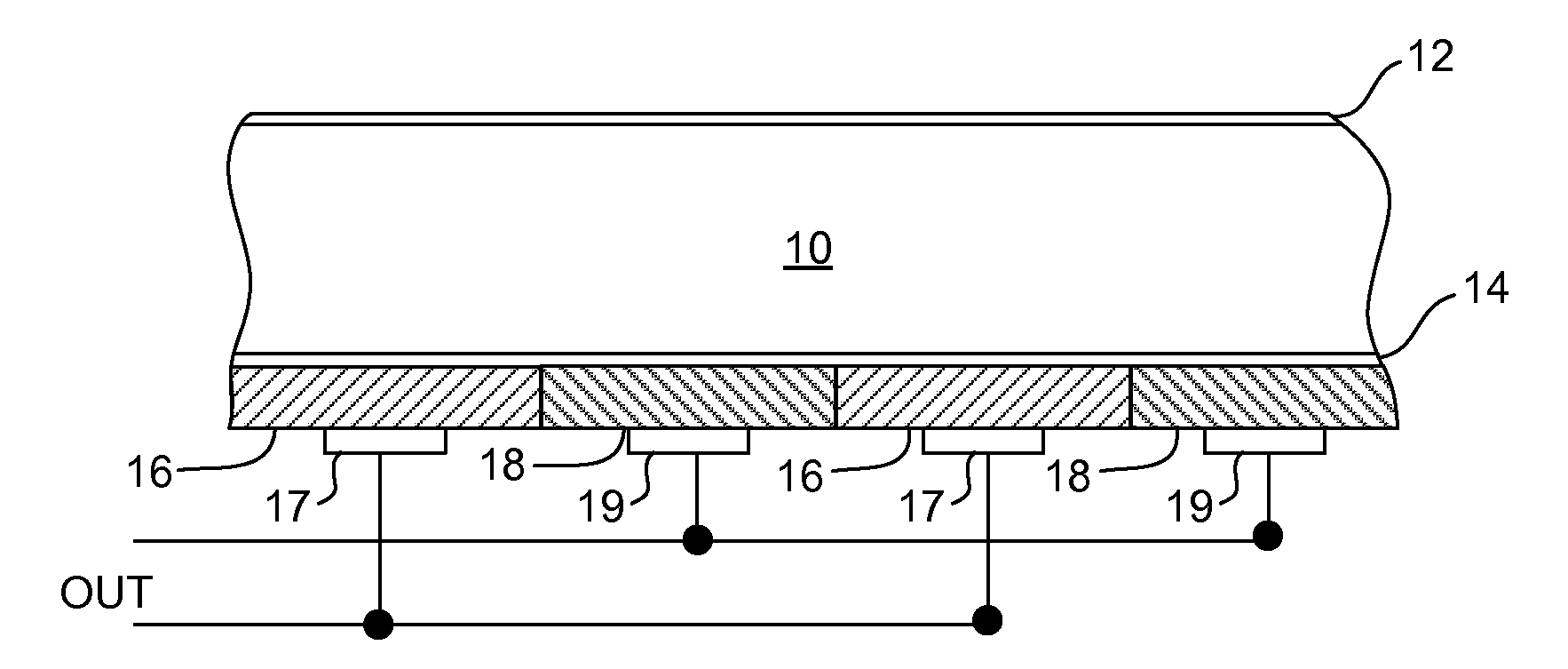
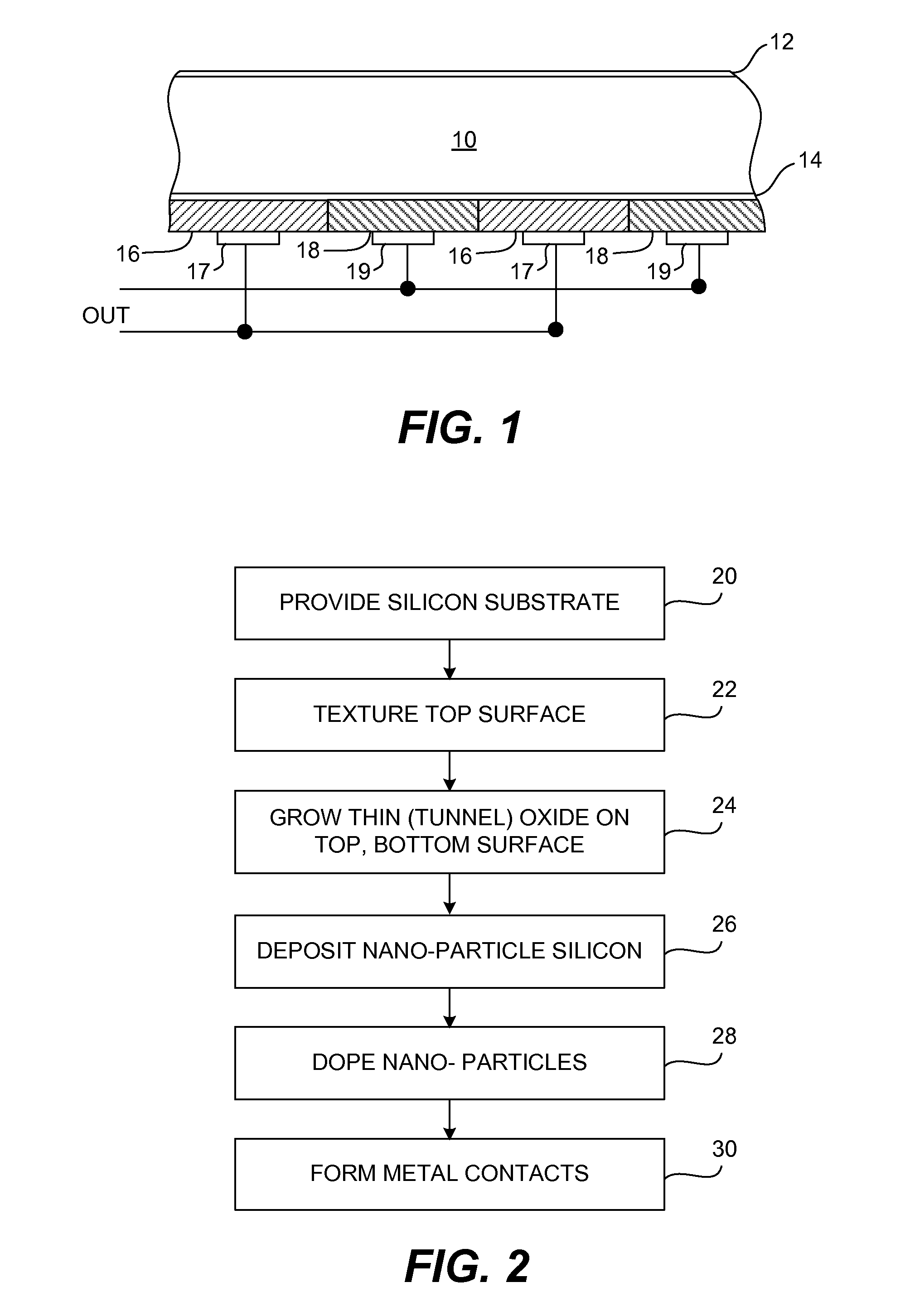
[0012]FIG. 1 illustrates in section view one embodiment of a solar cell in accordance with the invention. As in the conventional silicon solar cell, the cell comprises a polysilicon or single crystalline silicon substrate 10 with a thickness on the order of 200 microns and which can be either undoped or lightly doped (e.g. 5 ohm-centimeter). A passivation layer 12 is formed on the front surface of the substrate which can be textured by anisotropic texturing for example, prior to formation of the passivation layer. The passivation layer can be a thin silicon oxide layer which is grown simultaneously with a high quality tunnel oxide layer 14 on the bottom or back surface of substrate 10. The top passivation layer 12 can be coated with an anti-reflective coating such as silicon nitride or doped silicon carbide (not shown) as in conventional processing.

[0013]The back surface of substrate 10 includes alternating p-emitters 16 and n-emitters 18 which are formed by deposition over tunnel o...


PUM


Abstract

A silicon solar cell having a silicon substrate includes p-type and n-type emitters on a surface of the substrate, the emitters being doped nano-particles of silicon. To reduce high interface recombination at the substrate surface, the nano-particle emitters are preferably formed over a thin interfacial tunnel oxide layer on the surface of the substrate.

Description

BACKGROUND OF THE INVENTION[0001]This invention relates generally to photovoltaic solar cells, and more particularly the invention relates to a solar cell employing silicon nano-particle emitters.[0002]The use of photovoltaic cells for the direct conversion of solar radiation into electrical energy is well known, see Swanson, U.S. Pat. No. 4,234,352 for example. Briefly, the photovoltaic cell comprises a substrate of semiconductive material having a p-n junction defined therein. In the planar silicon cell the p-n junction is formed near a surface of the substrate which receives impinging radiation. Radiated photons create mobile carriers (holes and electrons) and the substrate which can be directed to an electrical circuit outside of the cell. Only photons having at least a minimum energy level (e.g., 1.1 electron volt for silicon) can generate an electron-hole pair in the semiconductor pair. Photons having less energy are either not absorbed or are absorbed as heat, and the excess ...

Claims


Application Information

Patent Timeline
Patent Type & Authority Applications(United States)
IPC IPC(8): H01L31/028H01L21/38
CPCH01L31/035281H01L31/061H01L31/18H01L31/035218Y02E10/50Y02E10/547H01L31/028H01L31/074
Inventor SWANSON, RICHARD M.
Owner MAXEON SOLAR PTE LTD
Why Eureka
Try Eureka