

Semiconductor device which has mos structure and method of manufacturing the same
a technology of mos structure and semiconductors, applied in the direction of semiconductor devices, electrical devices, transistors, etc., can solve the problems of complicated manufacturing process in the conventional device manufacturing method, and achieve the effect of simple manufacturing process and easy manufactur
- Summary
- Abstract
- Description
- Claims
- Application Information
AI Technical Summary
Benefits of technology
Problems solved by technology
Method used
Image

Examples
embodiment 1
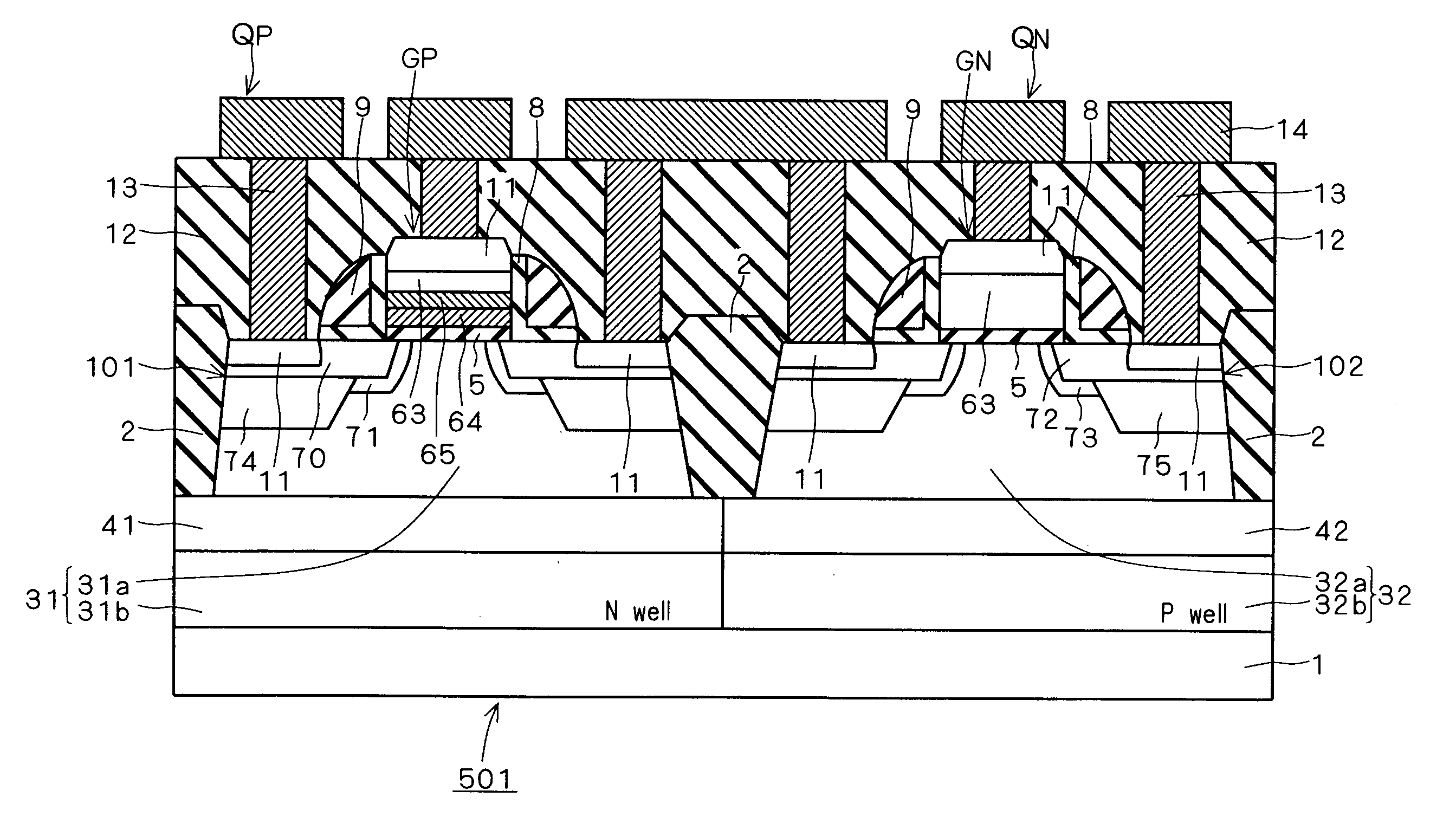
[0044]FIG. 1 is a cross-sectional view showing the structure of CMOS transistor 501 concerning this embodiment. CMOS transistor 501 is provided with PMOS transistor QP and NMOS transistor QN.
[0045]PMOS transistor QP is formed in N type well 31 (here, it can be grasped that N type well 31a is a first semiconductor layer). On the other hand, NMOS transistor QN is formed in P type well 32 (here, it can be grasped that P type well 32a is a second semiconductor layer). Both N type well 31 and P type well 32 are formed in one main surface (in FIG. 1, it is an upside) of semiconductor substrate 1. N type well 31a and P type well 32a are separated by element isolation insulator 2 (N type well 31b and P type well 32b are not separated by element isolation insulator 2 as FIG. 1 may show in addition). Semiconductor substrate 1, N type well 31, and P type well 32 all adopt silicon as the main ingredients, for example. Unless it refuses in particular, silicon is employable similarly about other ...
embodiment 2
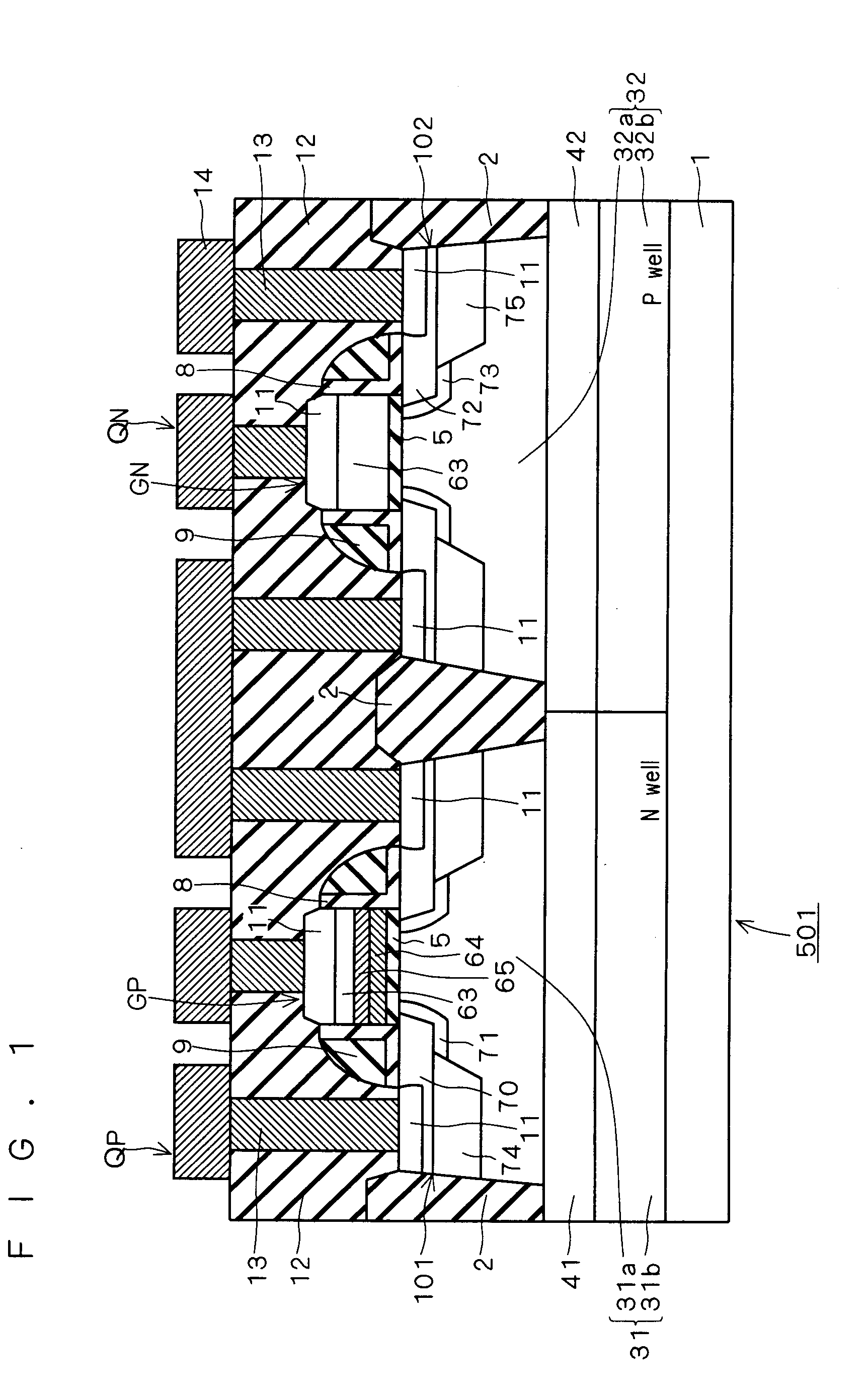
[0118]FIG. 16 is a cross-sectional view showing the structure of CMOS transistor 502 concerning this embodiment. CMOS transistor 502 is provided with PMOS transistor QP and NMOS transistor QN like Embodiment 1.
[0119]The structure except for transistors QP and QN (especially structure except for gate electrode GP and GN) is the same as that of CMOS transistor 501 (FIG. 1) explained by Embodiment 1 as it will be explained below. Therefore, explanation of structure that is common between Embodiment 1 and Embodiment 2 is omitted by this embodiment. In CMOS transistor 502, the same reference is attached about the same member as the member which forms CMOS transistor 501.
[0120]First, the structure of PMOS transistor QP concerning this embodiment is explained.
[0121]PMOS transistor QP has gate insulating film (it can be grasped as a first gate insulating film) 5 between gate electrode GP, and the channel region of N type well 31a. As gate insulating film 5 here, except for silicon oxide or ...
embodiment 3
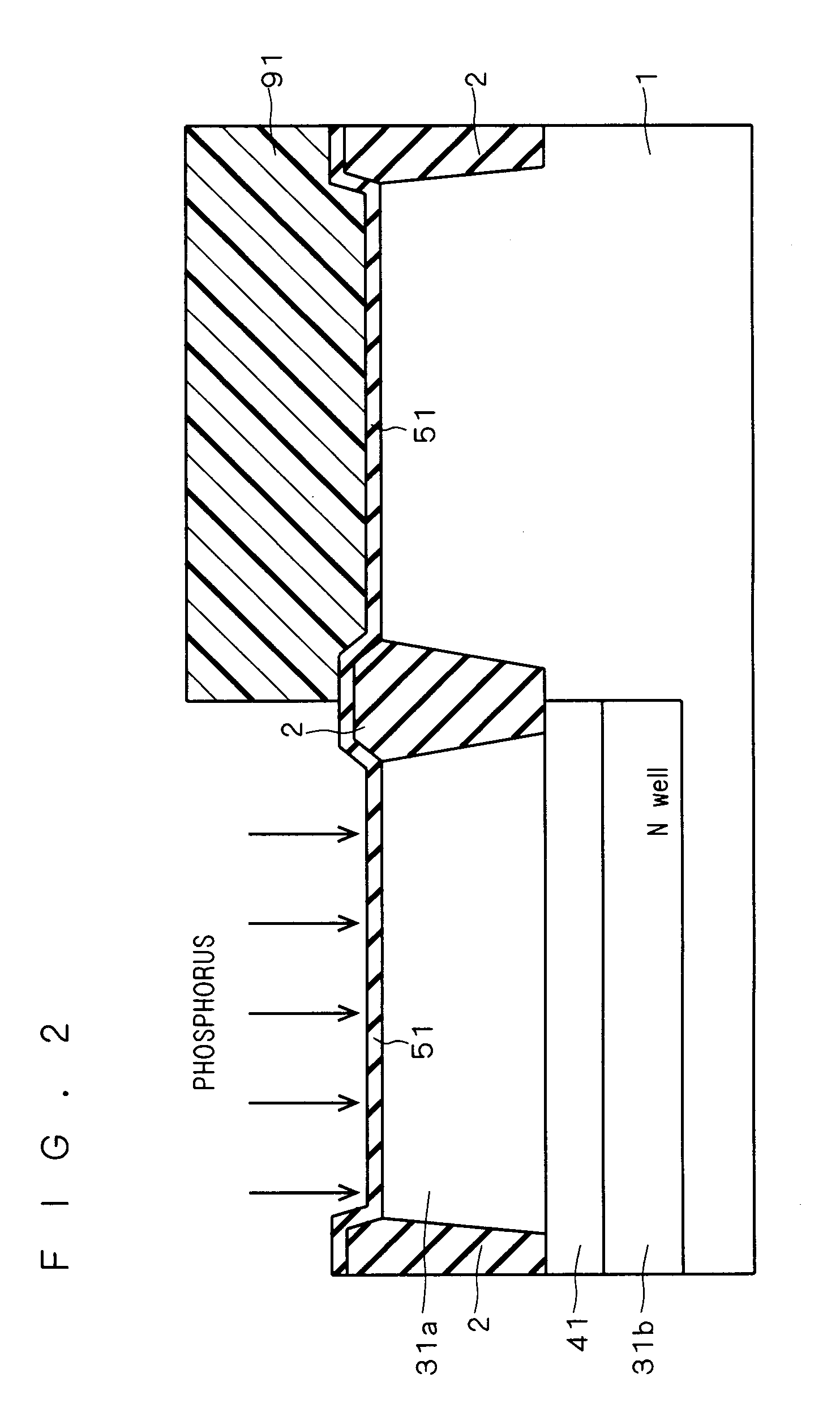
[0175]In Embodiment 1 and 2, in order to adjust threshold voltage (Vth) further, it described implanting a predetermined impurity into the substrate main surface of CMOS transistor 501,502 illustrated to FIG. 1 and 16. For example, in order to adjust the threshold voltage of PMOS transistor QP, halogen ion (fluorine ion) is implanted into the front surface of N type well 31a. In order to adjust the threshold voltage of NMOS transistor QN, nitrogen ion is implanted into the front surface of P type well 32a.
[0176]However, when its attention is paid only to the viewpoint of adjustment of the threshold voltage (Vth) by implanting impurity ion into a substrate main surface, the structure (concretely structure of a gate electrode) of the target CMOS transistor does not have the need of restricting to FIG. 1 and 16. Therefore, in this embodiment, reference is made about the form which implanted predetermined impurity ion into the front surface of the main surface of a substrate in which t...
PUM
 Abstract
Description
Claims
Application Information