Semiconductor Device And Production Method For Semiconductor Device

a semiconductor and production method technology, applied in the direction of semiconductor devices, semiconductor/solid-state device details, electrical apparatus, etc., can solve the problems of large chip load, rigid and brittle connection parts, and difficult to apply the above-described technologies to the die-mount connection part, etc., to achieve high connection reliability

Inactive Publication Date: 2008-05-29
RENESAS TECH CORP
View PDF1 Cites 25 Cited by
  • Summary
  • Abstract
  • Description
  • Claims
  • Application Information

AI Technical Summary

Benefits of technology

[0081]According to the present invention, in the case of reflow soldering of a material onto a substrate at the highest temperature of 260° C., it is possible to provide a Pb-free power semiconductor device with accompanying no flash of the solder in a die-mount-connection part and also a high connection reliability in the die-mount-connection part of a power semiconductor element and a lead frame in the power semiconductor device under the actual use environment even in the case where a thermal expansion coefficient difference is large between the materials to be connected.
[0082]As described above, according to the present invention, it is possible to conduct a Pb-free die-mount connection without causing any chip crack with respect to thermal stress, and with no melting of the solder in the case of reflowing.

Problems solved by technology

In the above-described two prior arts, however, there is no consideration as to the following points, so that it is difficult to apply the above-described technologies to the die-mount-connection part where is required to have high connection reliability for realizing an important function as a heat dissipation path for a power semiconductor element.
As a result, the connection part becomes rigid and brittle as compared with the existing high Pb solder.
In the case where the technologies of the non-patent documents 1 and 2 are applied to the junction of the combination of the power semiconductor element (Si) being the object of the present invention and a Cu-based lead frame exhibiting a large thermal expansion coefficient difference, the hard and brittle connection part as shown in the non-patent documents 1 and 2 cannot buffer the thermal stress produced in temperature cycles, resulting in a large load with respect to the chip thereby to cause chip cracks, and thus, the connection reliability cannot be assured.
Although it may be considered that a thickness of the connection part is increased as the measure for improving the prevention of chip cracks, the thickened connection part brings about a very long period of time for achieving a complete compound.
In this case, however, the remaining stress after the connection becomes large, and hence, it becomes a cause for generating chip cracks.

Method used


Image

  • Semiconductor Device And Production Method For Semiconductor Device
  • Semiconductor Device And Production Method For Semiconductor Device
  • Semiconductor Device And Production Method For Semiconductor Device

Examples


embodiment 1

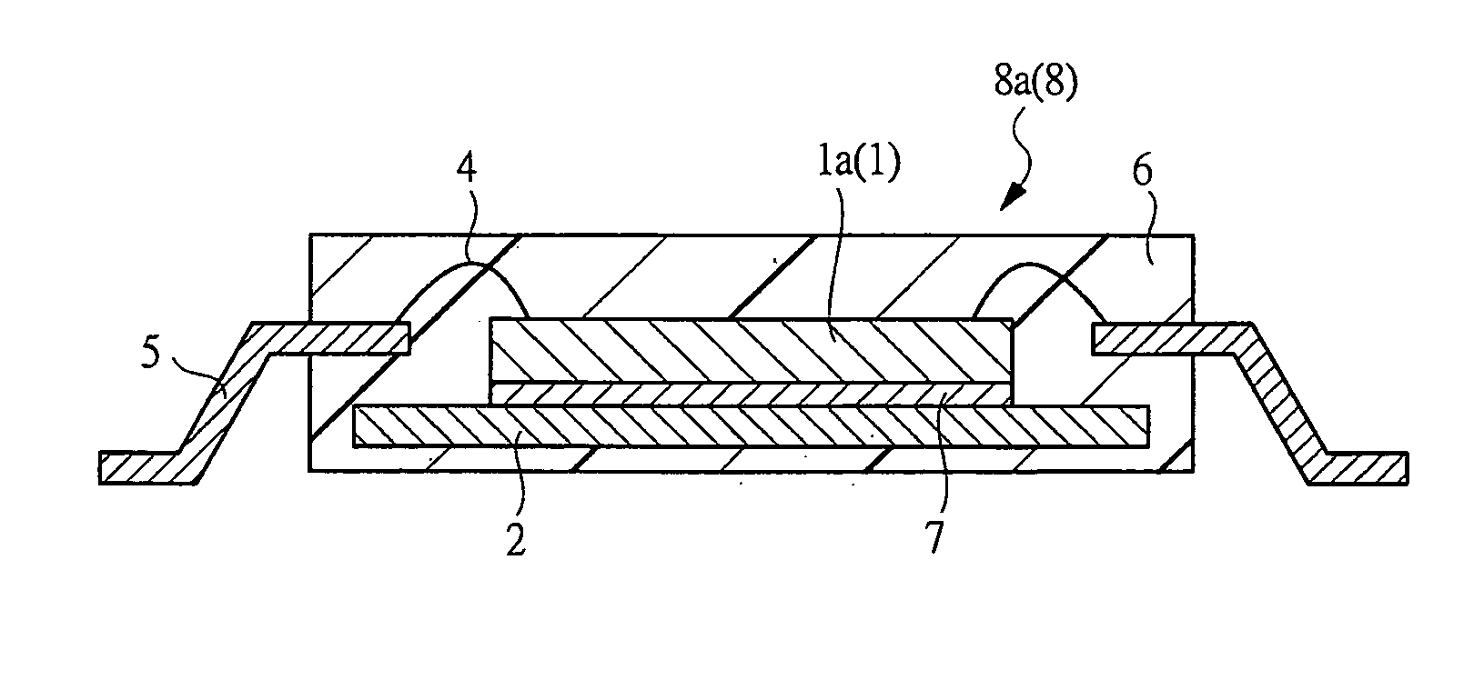
[0100]FIG. 4 is a sectional view showing a semiconductor device 8 according to an embodiment of the present invention wherein the semiconductor device 8 comprising a power semiconductor device 8a and the like is manufactured in accordance with, for example, the following manufacturing processes.

[0101]That is, as shown in FIG. 4, the power semiconductor device 8a is obtained by die-mount-connecting a semiconductor element 1 as a power semiconductor element 1a onto a lead frame 2 through a metal joint section 7. To form the metal joint section 7, a composite foil 7a for forming the joint section shown in FIG. 5A is disposed on a die pad of the lead frame 2, and further the power semiconductor device 8a is disposed on the composite foil 7a and heated.

[0102]For instance, on the rear surface on the silicon (Si) side of the power semiconductor element 1a being in contact with the composite foil 7a, Ti / Ni / Au is metallized to assure the wettability. The lead frame 2 is, for example, made of...

embodiment 2

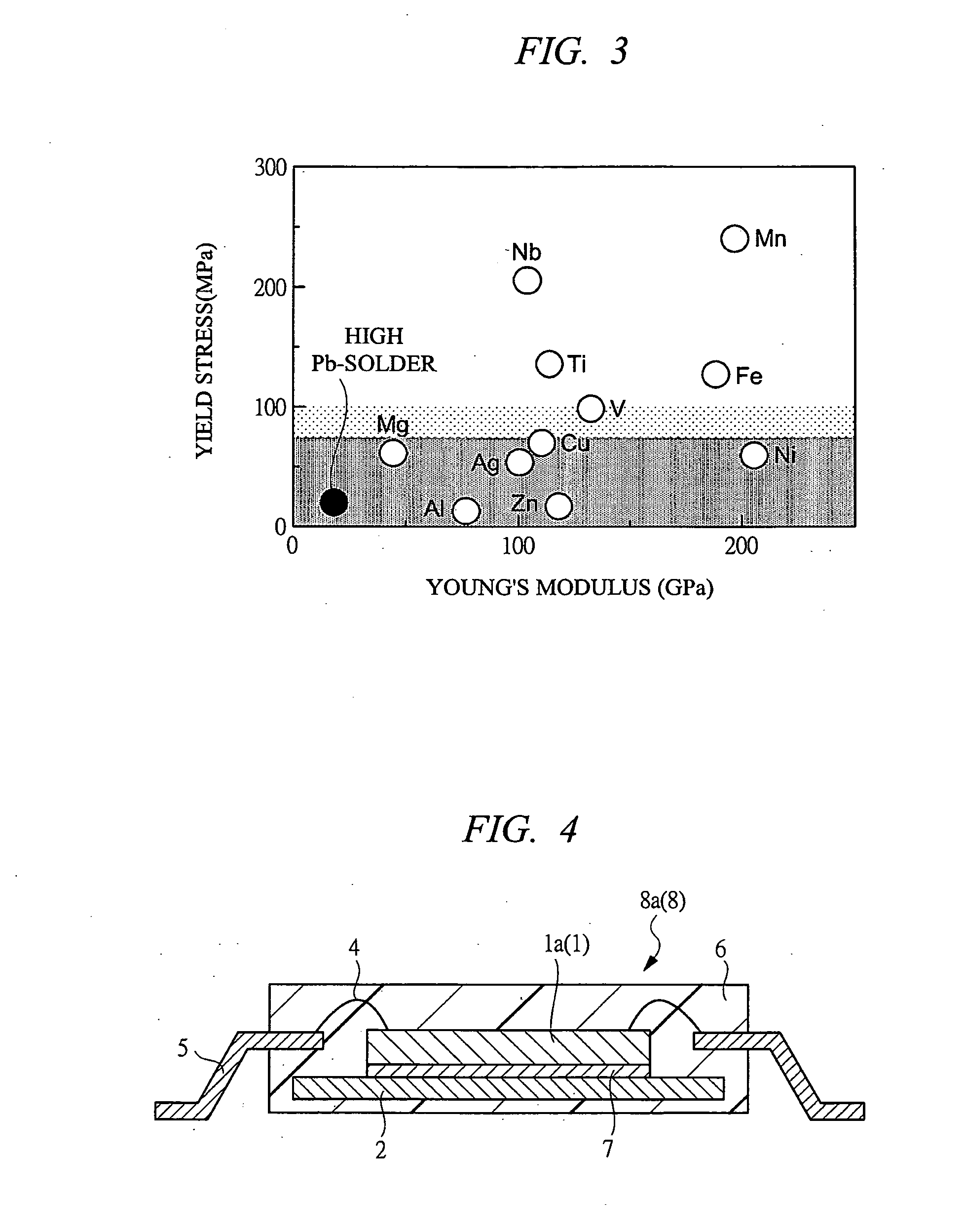
[0147]As is apparent from the above-described embodiment 1, such a construction which is not adversely affected, e.g. with appearance of cracks, by the rigid and brittle connection layer 200 and the side of the power semiconductor element 1a connected with the connection layer 200 may be obtained by the provision of the metal layer 100 wherein thermal stress is absorbed by the metal layer 100, even if the connection layer 200 comes to have a high melting point resulting in rigid and brittle characteristics.

[0148]In this connection, the present inventors get such an idea that when a Pb-free solder of a high melting point is used together with the metal layer 100, it becomes possible to use the Pb-free solder which could not have been used for the die-mount-connection because of occurrence of cracks by thermal stress on the chip side due to the rigid and brittle characteristics thereof although there is no fear of the remelting in the case of the reflow by making it to have a high mel...

embodiment 3

[0159]As is apparent from the above embodiment 1, such a construction which is not adversely affected, e.g. with appearance of cracks, by the rigid and brittle connection layer 200 and the side of the power semiconductor element 1a connected with the connection layer 200, may be obtained by the provision of the metal layer 100 wherein thermal stress is absorbed by the metal layer 100, even if the connection layer 200 comes to have a high melting point resulting in rigid and brittle characteristics.

[0160]In this connection, the present inventors get such an idea that when a Bi, a Bi—Ag alloy, a Bi—Cu alloy, or a Bi—Ag—Cu alloy-based solder is used together with the metal layer 100, it becomes possible to use any of these solders which could not have been used for the die-mount-connection because of occurrence of cracks by applying it thinly in spite of requiring the thin connection thereof due to its low thermal expansion coefficient of about 9 W / m·K, although there is no fear of the...


PUM

PropertyMeasurementUnit
melting pointaaaaaaaaaa
yield stressaaaaaaaaaa
melting pointaaaaaaaaaa

Abstract

A power semiconductor device in which a semiconductor element is die-mount-connected onto a lead frame in a Pb-free manner. In a die-mount-connection with a large difference of thermal expansion coefficient between a semiconductor element 1 and a lead frame 2, the connection is made with an intermetallic compound 200 having a melting point of 260° C. or higher or a Pb-free solder having a melting point of 260° C. or higher to 400° C. or lower, at the same time, the thermal stress produced in temperature cycles is buffered by a metal layer 100 having a melting point of 260° C. or higher. A Pb-free die-mount-connection which does not melt at the time of reflowing but have no chip crack to occur according to thermal stress can be achieved.

Description

TECHNICAL FIELD[0001]The present invention relates to a semiconductor device technology including a power semiconductor device having a die-mount-connection part connected with the use of a Pb(lead)-free metal composite foil.BACKGROUND ART[0002]A conventional power semiconductor device is shown in FIG. 1 wherein a power semiconductor element 1a is die-mount-connected onto a lead frame 2 by means a solder 3. After bonding the resulting product to leads 5 through wires 4, respectively, the bonded product is resin-molded with an epoxy-based resin 6. In this case, a high Pb solder and a solder to which trace amount of Ag or Cu are added to have a melting point (solidus temperature) of 290° C. or higher are used as the solder 3.[0003]In the wire bonding process, there is a case where the temperature becomes 280° C. at the maximum. Furthermore, when a power semiconductor device is surface-mount soldered to a substrate, it is supposed that the power semiconductor is heated up to 260° C. at...

Claims


Application Information

Patent Timeline
Patent Type & Authority Applications(United States)
IPC IPC(8): H01L23/495H01L21/52H01L21/60
CPCH01L2224/29101H01L2224/2908H01L2924/15747H01L24/45H01L2224/45124H01L2224/45144H01L2224/83192H01L2224/04026H01L2224/05111H01L2224/05139H01L2224/05147H01L2224/05155H01L2224/05166H01L2224/05171H01L2224/05644H01L2224/48644H01L2224/29083H01L2924/01014H01L23/49513H01L23/49524H01L23/49562H01L24/27H01L24/29H01L24/32H01L24/33H01L24/39H01L24/40H01L24/83H01L2224/29109H01L2224/29111H01L2224/32013H01L2224/32057H01L2224/32245H01L2224/32507H01L2224/48091H01L2224/48247H01L2224/73265H01L2224/83191H01L2224/83801H01L2224/92247H01L2924/01005H01L2924/01012H01L2924/01013H01L2924/01015H01L2924/01027H01L2924/01029H01L2924/0103H01L2924/01042H01L2924/01046H01L2924/01047H01L2924/01049H01L2924/0105H01L2924/01051H01L2924/01063H01L2924/01074H01L2924/01075H01L2924/01078H01L2924/01079H01L2924/01082H01L2924/01327H01L2924/10253H01L2924/10329H01L2924/13055H01L2224/29124H01L2224/29139H01L2224/29147H01L2924/01028H01L2224/29155H01L2224/29118H01L2224/29123H01L2924/0132H01L2924/0133H01L24/48H01L2224/2919H01L2224/83805H01L2924/01006H01L2924/01019H01L2924/01024H01L2924/01033H01L2924/01322H01L2924/014H01L2924/0665H01L2924/00014H01L2924/00H01L2924/01032H01L2924/00012H01L2924/01022H01L2924/01026H01L2924/01083H01L2924/3512H01L2224/48744H01L2924/00015H01L2224/48699H01L2224/37147H01L2224/40247H01L2924/1305H01L2924/351H01L2924/15787H01L2224/40095H01L2224/85205H01L2924/00011H01L2924/181H01L24/73H01L24/37H01L2224/84801H01L24/75H01L2224/2612H01L24/84H01L2224/83205H01L2224/73221
Inventor IKEDA, OSAMUOKAMOTO, MASAHIDEHARUTA, RYOKAGII, HIDEMASAOKA, HIROINAKAMURA, HIROYUKI
Owner RENESAS TECH CORP
Why Eureka
Try Eureka