On-Chip Spectroscopy

Active Publication Date: 2008-05-29
SERSTECH
View PDF2 Cites 42 Cited by
  • Summary
  • Abstract
  • Description
  • Claims
  • Application Information

AI Technical Summary

Benefits of technology

[0034]Especially, when using a silicon substrate, the light sensitive devices may be easily integrated with the substrate and the μTAS.
[0035]The interconnecting waveguide may be a multimode waveguide, thus the height of the waveguide may be selected so that multiple modes may be confined in the waveguide. It is an advantage of the system that the interconnecting waveguide may be selected to have the same height as the depth of the at least one microfluidic channel. Hereby may the microfluidic waveguide and the interconnecting waveguide be formed in one step without the need for additional steps reducing the he

Problems solved by technology

However, connection to external or off-chip active optical elements, such as light sources, detectors, spectroscopes, etc. is usually a demanding task, requiring precise alignment between the fluid handling chips and e.g.

Method used


Image

  • On-Chip Spectroscopy
  • On-Chip Spectroscopy
  • On-Chip Spectroscopy

Examples


Example

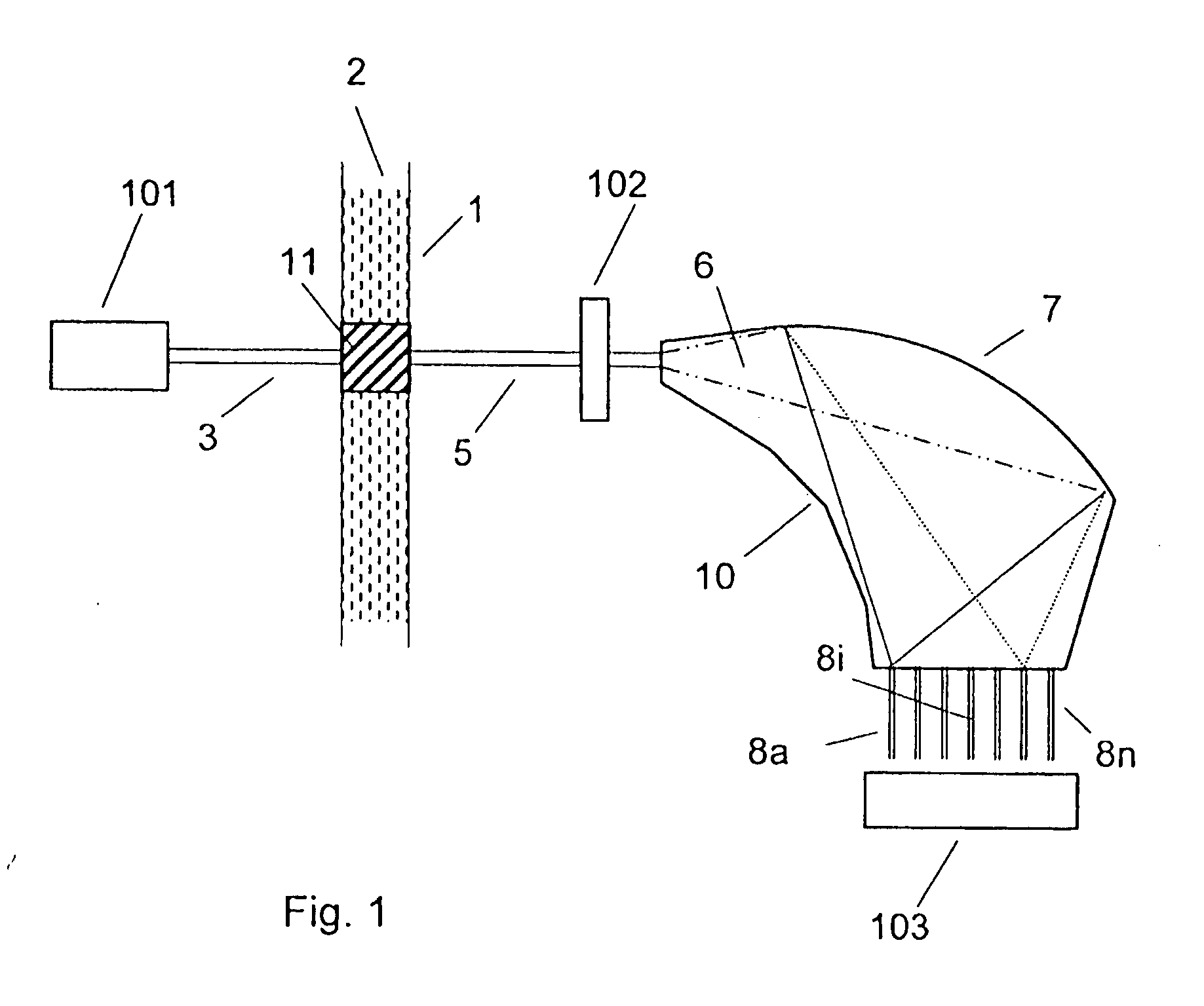
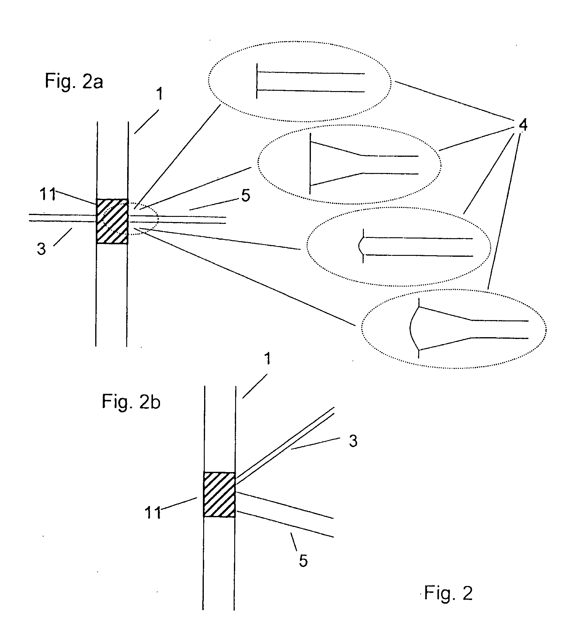
[0094]In FIG. 1, a micro total analysis system or at least a part of such a system is shown. The microfluidic channel 1 may comprise a fluid 2, being a gas or a liquid, to be analyzed.

[0095]The system in FIG. 1 is configured for absorption spectroscopy and a first optical waveguide 3 provides an incident electromagnetic wave to the fluid 2 in the analysation part 4, being substantially the exposed area of the channel. The incident electromagnetically wave is typically monochromatic light, such as a laser light. The electromagnetically wave may in a given embodiment be emitted from an external light source 101 or from a integrated light source 101. In a situation of fluorescence and Raman measurements may the electromagnetic wave also be launched through a transparent substrate or lid perpendicular to the channel 1. Typically, a part of the incident light will interact with the fluid and / or fluid components and be at least partly absorbed by the fluid or the fluid components. The res...


PUM

PropertyMeasurementUnit
Thicknessaaaaaaaaaa
Thicknessaaaaaaaaaa
Angleaaaaaaaaaa

Abstract

The present invention relates to a micro total analysis system comprising a spectroscope and a method of manufacturing such a system comprising a spectroscope in a one step process. More over the invention relates to a method of analyzing a sample in the system. The micro total analysis system comprising a spectroscope provided on a substrate and for measuring electromagnetic radiation and at least one microfluidic channel. The spectroscope comprises: a slab waveguide for guiding electromagnetic waves towards a diffraction grating dispersing the electromagnetic waves into their component wavelengths, and output means for receiving the deflected electromagnetic waves. At least a part of the microfluidic channel, the slab waveguide and the grating comprises the same main material, such as a polymer material.

Description

FIELD OF INVENTION[0001]The present invention relates to a micro total analysis system comprising a spectroscope and a method of manufacturing such a system comprising a spectroscope in a one step process.BACKGROUND OF THE INVENTION[0002]Micro total analysis systems (μTAS) are becoming more widely used, and further still more features are built into such systems. The systems may be used for fast analysis of small volumes of fluids. The micro systems comprise microfluidic channels and reaction chambers and also functional elements such as mixers, pumps and separation may be integrated on the chip. The detection of properties of fluids or fluid components is dominated by optical methods, such as fluorescence detection or absorption spectroscopy.[0003]Typically, the optical systems are provided at a separate device or only partly integrated with the fluid handling system. There has been a strong effort to integrate parts of the optical system, such as waveguides with the fluid handling...

Claims


Application Information

Patent Timeline
IPC IPC(8): G01J3/28C23F1/00G03F7/00B29C45/00B29C59/00B29C67/00B01L3/00G01J3/44G01N21/01G01N21/65
CPCG01J3/0256G01J3/18G01J3/28G01N2021/0346G01N21/05G01N21/645G01N21/658G01J3/44
Inventor HUBNER, JORGJORGENSEN, ANDERS MICHAELANHOJ, THOMAS AAROEZAUNER, DAN ANKER
Owner SERSTECH
Why Eureka
Try Eureka