Method Of Manufacturing Soi Wafer And Thus-Manufactured Soi Wafer

a manufacturing method and technology of soi wafer, which are applied in the direction of basic electric elements, electrical apparatus, semiconductor devices, etc., can solve the problems of affecting the quality of soi wafers, etc., to achieve rapid thermal processing, reduce the number of precipitation nuclei, and suppress the density of bmd formation

Active Publication Date: 2008-06-05
SHIN-ETSU HANDOTAI CO LTD
View PDF15 Cites 26 Cited by
  • Summary
  • Abstract
  • Description
  • Claims
  • Application Information

AI Technical Summary

Benefits of technology

[0032]It is now possible, prior to the bonding annealing, to carry out nuclei killer annealing for clearing the precipitation nuclei of the oxygen precipitate in the base wafer or reducing the density of the precipitation nuclei, to thereby fully reduce the number of precipitation nuclei possibly grown up to BMD during the bonding annealing, and to thereby readily suppress the density of formation of BMD in the base wafer of the resultant SOI wafer to less than 1×10⁹ / cm3. The nuclei killer annealing is necessarily carried out so as to heat the wafer up to the target temperature at a temperature elevation speed larger than that in the bonding annealing. The hold temperature during the annealing is preferably set to 900° C. to 1,200° C., both ends inclusive. The temperature lower than 900° C. may make it difficult to fully re-solubilize into sold and clear the precipitation nuclei, and the annealing at a temperature exceeding 1,200° C. may make slip dislocation more likely to occur. The heating up to the hold temperature in the annealing is preferably carried out at a temperature elevation speed of 5° C. / second to 100° C. / second, both ends inclusive. The temperature elevation speed of less than 5° C. / second may raise a fear of growing up of the precipitation nuclei to BMD, whereas the temperature elevation speed exceeding 100° C. / second is less feasible for normal annealing apparatus. The nuclei killer annealing raising such needs of temperature elevation speed is preferably carried out using a single-wafer-processing type rapid thermal processing (RTP) apparatus based on infrared lamp heating. The heating is preferably carried out using infrared lamps, so as to simultaneously heat both surfaces of the SOI wafer, wherein heating of only a single surface is also allowable.
[0033]A hydrogen atmosphere, an Ar atmosphere, or a mixed atmosphere of the both, for example, is applicable to the atmosphere for the nuclei killer annealing. The hold temperature in the annealing for this case is preferably set to 900° C. to 1,100° C., both ends inclusive. This is because, when the hydrogen atmosphere or the Ar atmosphere is adopted, the annealing above 1,100° C. may promote introduction of atomic vacancy (capable of mediating diffusion in the process of oxygen precipitation) into silicon single crystal during the annealing, and may rather increase the density of formation of BMD. On the other hand, the nuclei killer annealing may be carried out also in an oxygen atmosphere. Introduction of atomic vacancy is suppressed under the oxygen atmosphere, so that a target of the hold temperature in the annealing can be set to 900° C. to 1,200° C., both ends inclusive, as being expanded larger on the high temperature side.

Problems solved by technology

Conventional SOI wafers have suffered from a drawback in that they are likely to cause warping of the substrate, due to difference in thermal expansion coefficients between the base wafer and the SOI layer composed of silicon single crystal, and the silicon oxide layer.
If the warping of the SOI wafer increases, focusing in photolithographic process may become difficult, and device formation consequently becomes difficult.
The drawback will be more distinct as the degree of integration of integrated circuits increases.

Method used


Image

  • Method Of Manufacturing Soi Wafer And Thus-Manufactured Soi Wafer
  • Method Of Manufacturing Soi Wafer And Thus-Manufactured Soi Wafer
  • Method Of Manufacturing Soi Wafer And Thus-Manufactured Soi Wafer

Examples


embodiment

Second Mode of Embodiment

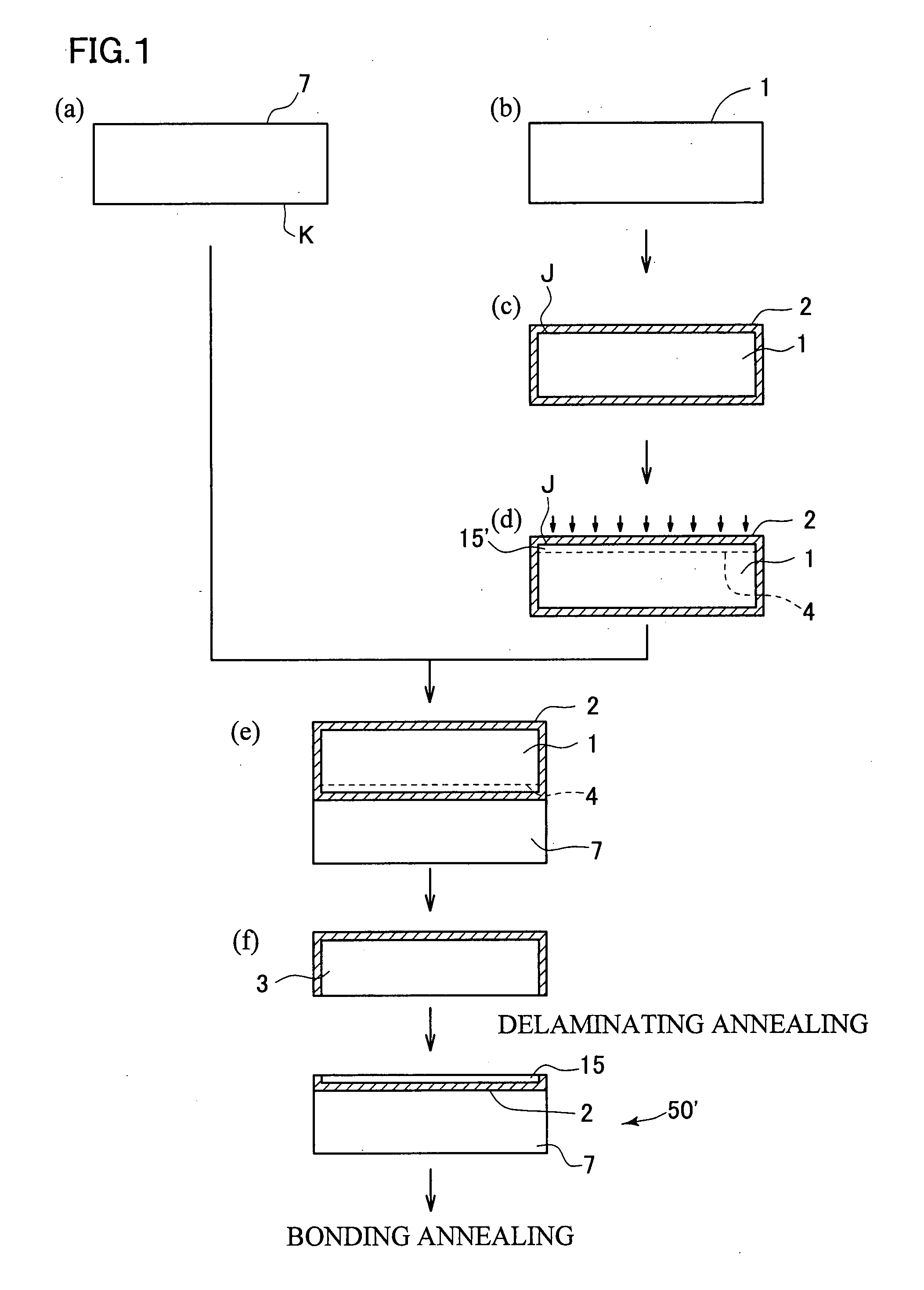
[0074]The SOI wafers after completion of the bonding annealing and therefore having a large number of BMD formed in the base wafers can be subjected to the precipitate clearing annealing aimed at reducing the density of formation of the BMD. First, prior to the precipitate clearing annealing, an oxide film on the surface of the SOI wafer is removed, and then subjected to a process step for removing a damaged layer and surface roughness of the SOI layer. It is known that fabrication of SOI wafers by the ion implantation delamination method produces a damaged layer and surface roughness, when ion implantation is carried out, remained in the surficial portion of the SOI layer. It is therefore a general practice to remove the damaged layer and surface roughness formed in the SOI layer after completion of the bonding annealing. A method of annealing in an inert gas such as Ar gas, or hydrogen gas, or a mixed gas of the both is adoptable to the removal step. The a...


PUM

PropertyMeasurementUnit
peak wavelengthaaaaaaaaaa
hold temperatureaaaaaaaaaa
temperatureaaaaaaaaaa

Abstract

A method of manufacturing an SOI wafer includes a bonding step, a thinning and a bonding annealing step. Assuming refractive index n1 of SiO2 as 1.5, refractive index n2 of Si as 3.5, and optical thickness tOP of the silicon oxide film 2 and the SOI layer 15 in the infrared wavelength region as tOP=n1×t1+n2×t2, the thickness t1 of the silicon oxide film 2 and thickness t2 of the SOI layer so as to satisfy a relation of 0.1λ<tOP<2λ, and so as to make (tn1)/(t2×n2) fall within 0.2 to 3. By nuclei killer annealing carried out before the bonding annealing, density of formation of oxygen precipitate in the base wafer after the bonding annealing is adjusted to less than 1×10⁹/cm3. This configuration successfully provides a method of manufacturing the SOI wafer having the thin silicon oxide film and the SOI layer, and being less likely to cause warping.

Description

RELATED APPLICATIONS[0001]This application claims the priorities of Japanese Patent Application No. 2004-265901 filed on Sep. 13, 2004 and No. 2004-268901 filed on Sep. 15, 2004, which are incorporated herein by reference.BACKGROUND OF THE INVENTION[0002]1. Field of the Invention[0003]This invention relates to a method of manufacturing an SOI wafer, and thus-manufactured SOI wafer.[0004]2. Description of the Related Art[0005]Patent Document 1: Japanese Laid-Open Patent Publication No. H9-64319[0006]So-called SOI wafers, obtained by forming a silicon oxide film on a silicon single crystal substrate (also referred to as “base wafer”, hereinafter), and by forming another silicon single crystal layer as being stacked thereon as an SOI (silicon on insulator) layer, are used for manufacturing semiconductor devices such as CMOS-IC and high-withstand-voltage-type IC. Bonding process, the SIMOX process and so forth are known as methods for manufacturing the SOI wafers. The bonding method is ...

Claims


Application Information

Patent Timeline
Patent Type & Authority Applications(United States)
IPC IPC(8): H01L29/00H01L21/30
CPCH01L21/76254H01L21/3226H01L27/12H01L21/02
Inventor AGA, HIROJIKOBAYASHI, NORIHIROIMAI, MASAYUKIENOMOTO, TATSUOTAKENO, HIROSHI
Owner SHIN-ETSU HANDOTAI CO LTD
Why Eureka
Try Eureka