Semiconductor Device

a technology of semiconductor devices and semiconductor chips, applied in the direction of solid-state devices, printed circuit manufacturing, basic electric elements, etc., can solve the problems of reducing the connection reliability of semiconductor devices, reducing the strength of junction portions, etc., and achieve the effect of suppressing the disconnection between a package substrate and a mounting substrate, reducing the stress concentration of the peripheral part of the package substrate, and reducing the stress concentration of the connection portion of the solder bump and the semiconductor chip

Inactive Publication Date: 2008-06-05
RENESAS ELECTRONICS CORP
View PDF2 Cites 16 Cited by
  • Summary
  • Abstract
  • Description
  • Claims
  • Application Information

AI Technical Summary

Benefits of technology

[0015]According to the semiconductor device concerning the present invention, since the elastic modulus is low, the inner bump can buffer the stress resulting from the difference in the coefficient of thermal expansion of a solder bump and under-filling resin. Therefore, the stress concentration to the connection portion of a solder bump and a semiconductor chip and the connection portion of a solder bump and a package substrate can be eased. Since the elastic modulus is high, the solder ball can hold the stress applied from the outside as self internal stress. Therefore, a solder ball can absorb the stress resulting from the difference in the coefficient of thermal expansion of a package substrate, and the mounting substrate which does external connection at the time of mounting, and the stress concentration to the peripheral part of a package substrate is eased. Therefore, disconnection between a package substrate and a mounting substrate can be suppressed. As a result, the connection reliability of the internal wiring of a semiconductor device and the connection reliability with external wiring at the time of mounting can be improved.
[0016]The purpose, the feature, aspect, and advantage of this invention become clearer with the following detailed explanation and accompanying drawings.

Problems solved by technology

Therefore, a solder bump's volume and the junction area of a solder bump and a pad will become small inevitably, and the strength of a junction portion will fall.
The stress was applied to the inner bump or the outer ball, became a factor which causes disconnection, and was reducing the connection reliability of the semiconductor device.

Method used


Image

  • Semiconductor Device
  • Semiconductor Device
  • Semiconductor Device

Examples


Embodiment Construction

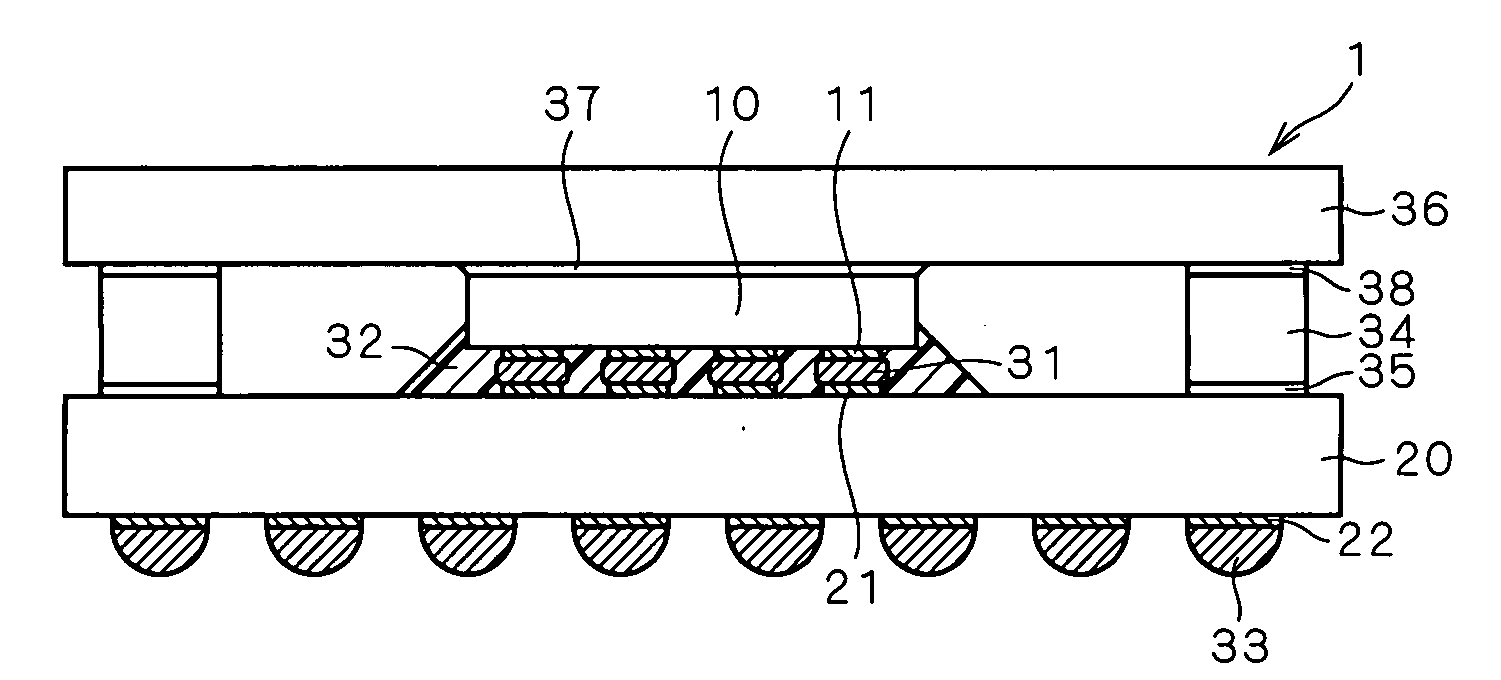
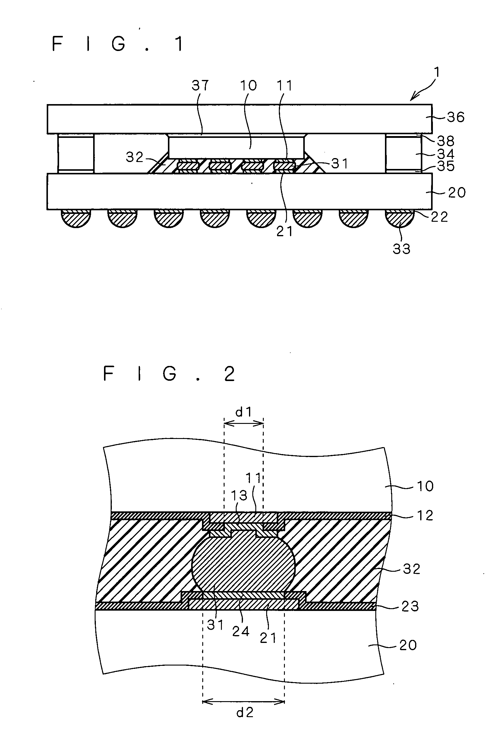
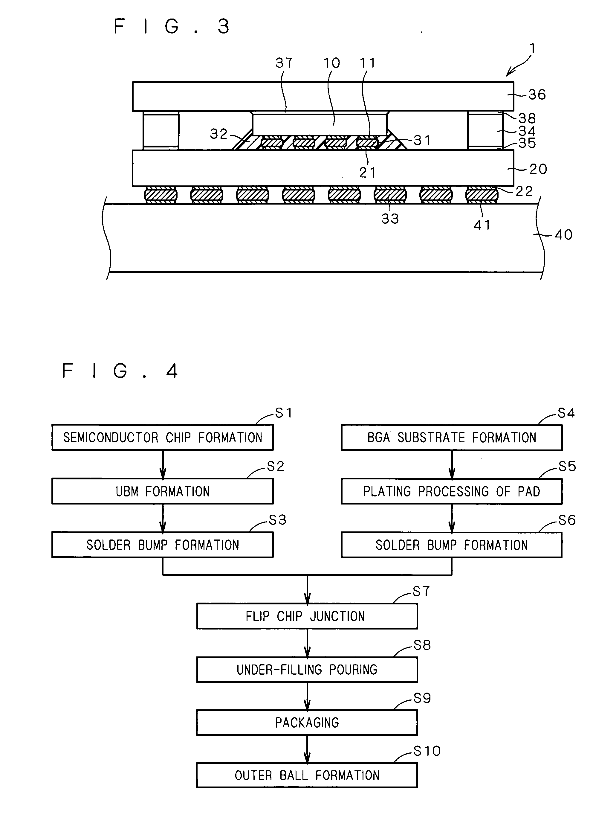
[0022]FIG. 1 is a drawing showing the structure of the semiconductor device concerning an embodiment of the invention. The semiconductor device 1 concerned has BGA structure, and BGA substrate (package substrate) 20 is equipped with semiconductor chip 10 by the face down method. On the under surface (integrated circuit surface), semiconductor chip 10 has a plurality of first pads 11. BGA substrate 20 has a plurality of second pads 21 as an internal electrode on the upper surface (mounting surface of semiconductor 1 chip). Both first pad 11 and second pad 21 are connected to solder bump (inner bump) 31 electrically and mechanically. Thereby, it electrically connects with BGA substrate 20, and semiconductor chip 10 is fixed mechanically.

[0023]The gap of semiconductor chip 10 and BGA substrate 20 is filled up with under-filling resin 32, such as an epoxy resin. Under-filling resin 32 pastes up between semiconductor chip 10 and BGA substrates 20, and it functions as easing the external ...


PUM


Abstract

Regarding a semiconductor device, especially the present invention suppresses disconnection of the connection structure concerned in the semiconductor device which has the electric and mechanical connection structure using solder, and aims at improving connection reliability. And to achieve the above objects, the semiconductor device has the solder bump which electrically connects a semiconductor chip and a package substrate, the under-filling resin with which it filled up between the semiconductor chip and the package substrate, and a solder ball which electrically connects a package substrate with the outside, and the solder bump's elastic modulus is made lower than the elastic modulus of a solder ball.

Description

INCORPORATION BY REFERENCE[0001]The present application claims priority from PCT application PCT / JP2004 / 018579 filed on Dec. 13, 2004, the content of which is hereby incorporated by reference into this application.TECHNICAL FIELD[0002]The present invention relates to a semiconductor device and relates to the semiconductor device which has the electric and mechanical connection structure using solder especially.BACKGROUND ART[0003]Flip chip bonding is known as one of the assembly technology of a semiconductor device. This bonding method is a method which sticks the connection pad (only henceforth a “pad”) formed in the under surface of the semiconductor chip, and the pad formed in the package substrate upper surface, applies heat and pressure, and is joined. On each pad of a semiconductor chip and a package substrate, the solder bump of ball state is beforehand formed in the case. Usually, the solder bump is put in order in a lattice manner, and such a structure is called BGA (Ball G...

Claims


Application Information

Patent Timeline
Patent Type & Authority Applications(United States)
IPC IPC(8): H01L23/488
CPCH01L21/563H01L23/36H01L24/13H01L2224/92125H01L2224/73204H01L2224/32225H01L2224/16225H01L2924/014H01L2924/01047H01L2924/01033H01L2924/01006H01L2924/01005H05K3/3463H05K3/3436H05K1/141H01L2924/16195H01L2924/15311H01L23/49816H01L24/10H01L2224/13099H01L2224/16H01L2224/73203H01L2224/73253H01L2924/01013H01L2924/01022H01L2924/01029H01L2924/01078H01L2924/01079H01L2924/01082H01L2924/01322H01L2924/14H01L2924/00H01L2924/181H01L2224/13H01L2224/05022H01L2224/05001H01L2224/05572H01L2224/05124H01L2224/05147H01L2224/05166H01L2224/05666H01L24/05H01L24/03H01L2224/16237H01L2924/00014
Inventor HAYASHI, EIJI
Owner RENESAS ELECTRONICS CORP
Why Eureka
Try Eureka