Semiconductor device and method of designing semiconductor device

a semiconductor device and semiconductor technology, applied in the field of semiconductor devices, can solve the problems of omitting the step of providing delay buffers, useless function in the conventional design method, etc., and achieve the effects of reducing the development term, reducing the area, and reducing power consumption

Inactive Publication Date: 2008-06-05
PANASONIC CORP
View PDF9 Cites 18 Cited by
  • Summary
  • Abstract
  • Description
  • Claims
  • Application Information

AI Technical Summary

Benefits of technology

[0018]The present invention has been made to solve the above-described problems, and therefore, has an object to provide a semiconductor device capable of simultaneously realizing low power consumption, a reduction of a developing term, a reduction of an area, and a high-speed operation, and also to provide a method for designing the semiconductor device.
[0020]The above-described designing method has an initial condition that while the clock signal having the single phase is not supplied which has been performed in the conventional designing method, clock signals having multiple phases are supplied. Also, while a Skew target value when CTS is designed is not selected to be zero, the semiconductor device is designed in such a manner that such clock signal phases having the smallest time difference value are selected to be supplied in coincident with timing of transmission / reception time (will also be referred to as “propagation time” hereinafter) on the data sides between the flip-flops. As a consequence, it is possible to omit the step for providing the delay buffers which have been inserted only for the timing adjustment and have the useless function in the conventional designing method. Accordingly, in accordance with the designing method of the present invention, both the CTS manner which is necessarily required in the timing design, and also, the transmission / reception timing as to the clock signals and the data among the flip-flops can be effectively designed.
[0022]As a result, the timing can be more effectively adjusted.
[0024]As a consequence, the timing design margin made by considering the local voltage drop of the power supply when the semiconductor device is operated can be decreased, and the current supply capability of the regulator which is mounted at the same time on the product can be reduced, so that the entire cost of the semiconductor device (system) can be lowered.
[0030]With employment of the above-described arrangement, the clock signal may be supplied under stable condition without receiving adverse influences caused by a temperature characteristic and a voltage characteristic.
[0033]According to the present invention, it is possible to provide such a semiconductor device capable of simultaneously realizing the low power consumption, the reduction of the developing term, the reduction of the area, and the high-speed operation, and also to provide such a method for designing the semiconductor device.

Problems solved by technology

As a consequence, it is possible to omit the step for providing the delay buffers which have been inserted only for the timing adjustment and have the useless function in the conventional designing method.

Method used


Image

  • Semiconductor device and method of designing semiconductor device
  • Semiconductor device and method of designing semiconductor device
  • Semiconductor device and method of designing semiconductor device

Examples


embodiment mode 1

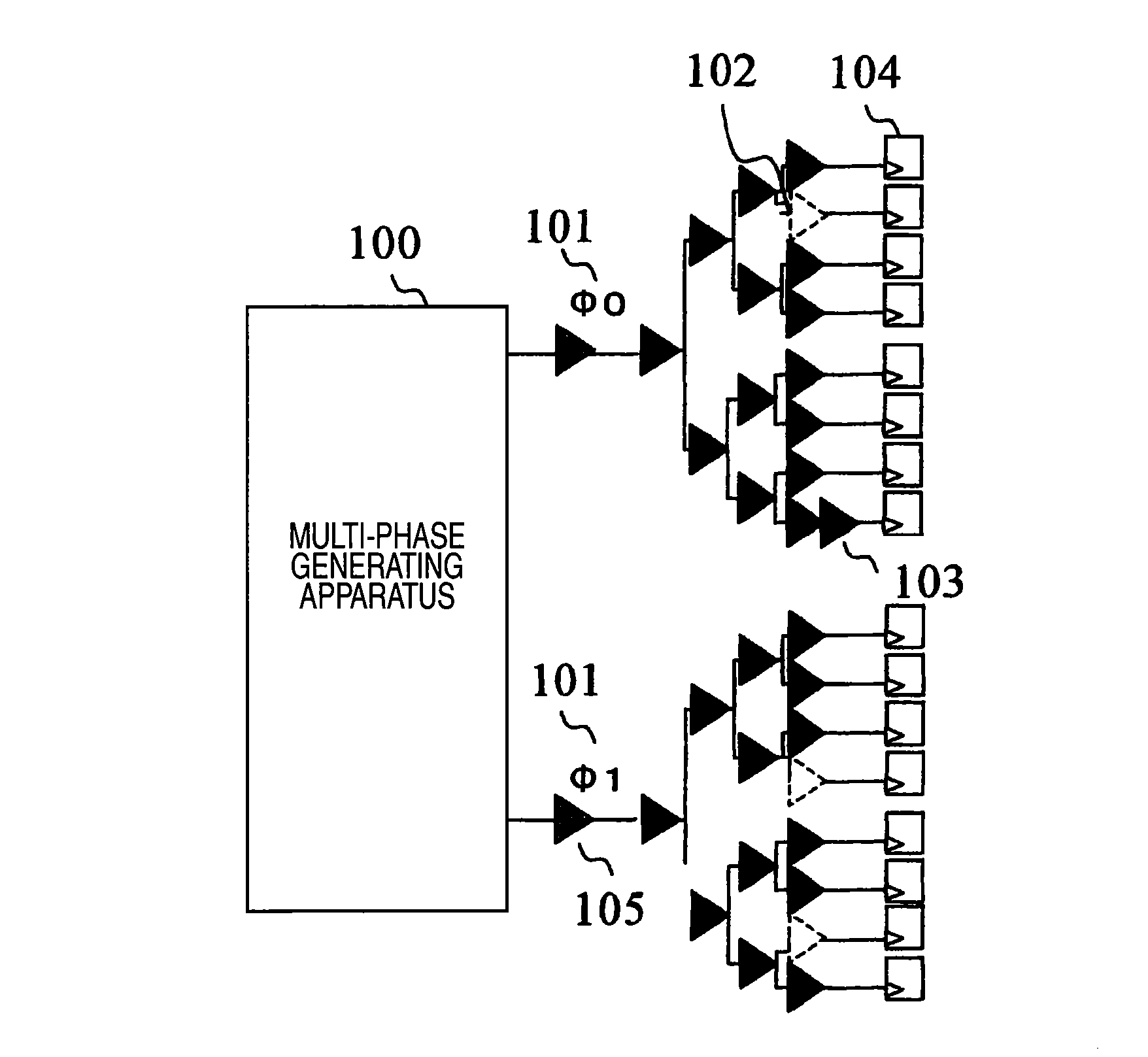
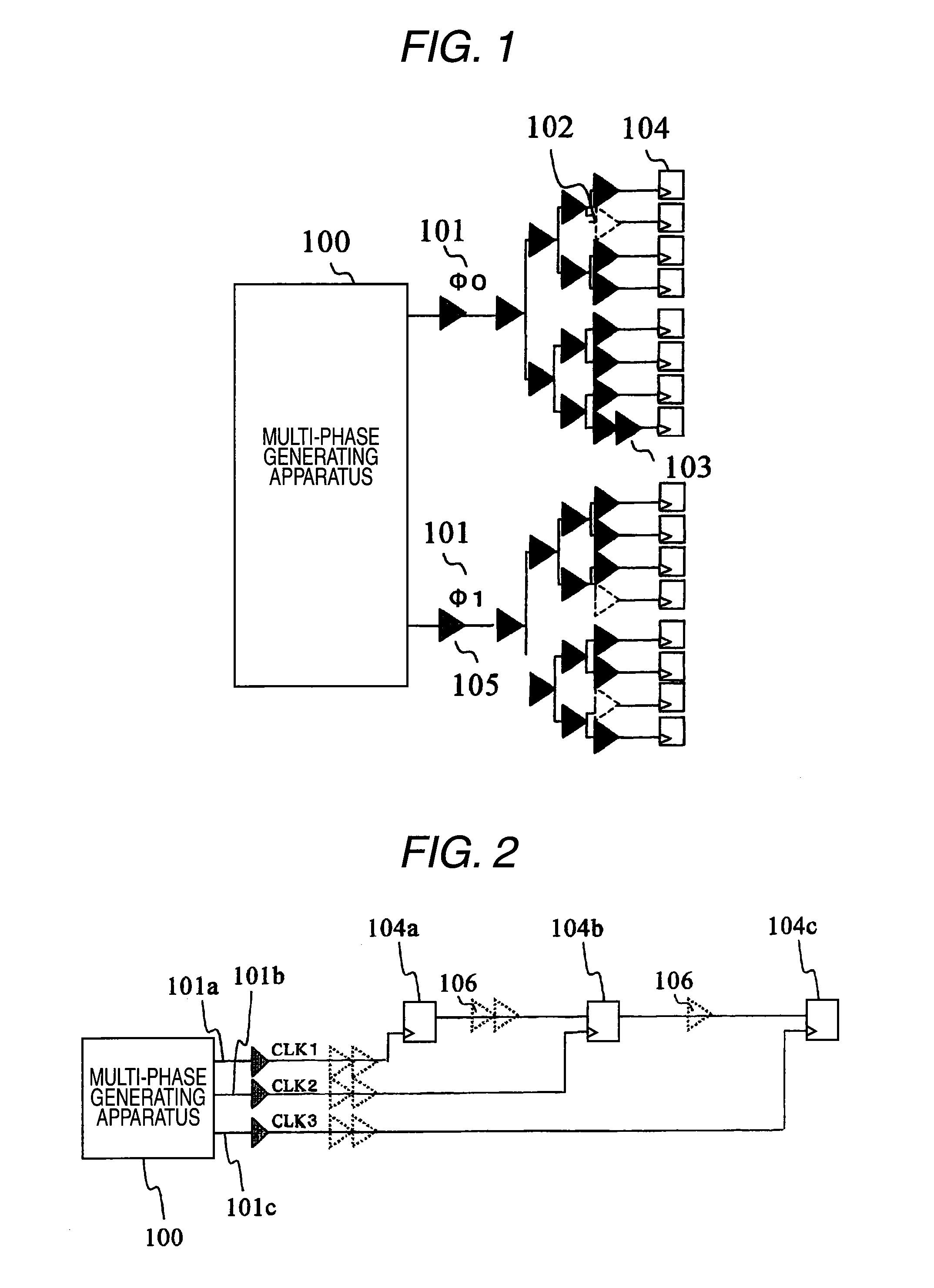
[0046]A description is made of a method for designing a semiconductor device according to an embodiment mode 1 of the present invention. Firstly, a description is made of a clock tree which is employed in the method for designing the semiconductor device according to the embodiment mode 1. FIG. 1 is a diagram for showing a schematic structure of the clock tree which is employed in the method for designing the semiconductor device according to the embodiment mode 1. A multi-phase generating apparatus 100 shown in FIG. 1 is capable of supplying clock signals having a plurality of phases, and is used in order to supply clock signals having optimum phases within an adjustable range by considering propagation times on the data sides of flip-flops. The way for adjustments will be discussed later.

[0047]Reference numeral 101 indicated in FIG. 1 represents phases of plural clock signals which are supplied from the multi-phase generating apparatus 100. In addition to a method for adjusting a ...

embodiment mode 2

[0064]Next, a description is made of a method for designing a semiconductor device, according to an embodiment mode 2 of the present invention. It should be noted that the same reference numerals shown in the above-described embodiment mode 1 will be employed as those for denoting the same structural elements indicated in the embodiment mode 2, and therefore, detailed explanations thereof will be omitted. FIG. 6 is an explanatory diagram for explaining a reduction of peak power. FIG. 7 is a schematic structural diagram of the semiconductor device which is designed based upon the designing method of the embodiment mode 2. FIG. 8 show a relationship diagram between the semiconductor device of FIG. 7 and a regulator.

[0065]In FIG. 6, reference numeral 250 shows a peak current value as to an initial condition of a clock signal phase. Reference numeral 251 represents a distributed peak current value. In FIG. 7, reference numerals 252a, 252b, 252c, 252d, and 252e indicate flip-flops, respe...

embodiment mode 3

[0070]Next, a description is made of a method for designing a semiconductor device, according to an embodiment mode 3 of the present invention. It should be noted that the same reference numerals shown in the above-described embodiment mode 1 will be employed as those for denoting the same structural elements indicated in the embodiment mode 3, and therefore, detailed explanations thereof will be omitted.

[0071]FIG. 9 graphically represents all of timing “Slack.”FIG. 10 shows a schematic structural diagram of a semiconductor device which has been designed in accordance with the designing method of the embodiment mode 3. In FIG. 9, reference numeral 200 indicates timing checked values under the worst condition, namely, a left-sided timing checked value indicates a “margin”, whereas a right-sided timing checked value indicates a “violation.” Reference numeral 201 indicates timing checked values under the Typ condition, namely, a left-sided timing checked value indicates a “margin”, whe...


PUM


Abstract

A semiconductor device designing method of the present invention corresponds to a method for designing a clock synthesization type semiconductor device, which is comprised of: a rough CTS (clock tree synthesis) step for performing the CTS within an adjustable range in multiple phases; a timing check step for judging whether or not transmission / reception of data are carried out under normal condition based upon a propagation time of data and an arrival time of a clock signal between flip-flops; a detailed timing analyzing step for judging whether or not the transmission / reception of the data can be carried out under the normal condition by switching a phase of a clock signal, or by increasing / decreasing a buffer in a half way of the clock tree as to supply timing of the clock signal; and a re-allocating step of a CLK net, for allocating a phase of such a clock signal which does not cause a timing violation every flip-flop based upon the result of the detailed timing analyzing step.

Description

BACKGROUND OF THE INVENTION[0001]1. Field of the Invention[0002]The present invention generally relates to a semiconductor device. More specifically, the present invention is directed to a semiconductor device capable of simultaneously realizing low power consumption, a reduction of a developing term, a reduction of an area, and a high-speed operation, and also directed to a method for designing the semiconductor device.[0003]2. Description of the Related Art[0004]Very recently, semiconductor devices have been manufactured in very fine manners, so that structures of these semiconductor devices have become complex, developing terms of the semiconductor devices have been prolonged, and these semiconductor devices have been equipped with higher functions. On the other hand, in order to accept requirements of high-speed operations, in method for designing semiconductor devices with employment of CMOS circuits, there are various contrary requirements, for instance, high-speed operation a...

Claims


Application Information

Patent Timeline
Patent Type & Authority Applications(United States)
IPC IPC(8): G06F1/04G06F17/50
CPCG06F17/5031G06F1/10G06F30/3312
Inventor KAWAI, TADAYUKI
Owner PANASONIC CORP
Why Eureka
Try Eureka