Display panel and film therefor

a technology of display panel and film, which is applied in the field of display panel, can solve the problems of inefficient productivity and cost effectiveness, production line cannot be operated at a high speed, and defects caused by contaminated foreign matter or flaws may become more frequent, so as to improve productivity, prevent defects caused by contaminated foreign matter or flaws, and reduce the thickness of the filter

Inactive Publication Date: 2008-06-05
BRIDGESTONE CORP
View PDF3 Cites 8 Cited by
  • Summary
  • Abstract
  • Description
  • Claims
  • Application Information

AI Technical Summary

Benefits of technology

[0008]The display panel film of the present invention includes a near-infrared absorption layer, a conductive layer, and an antireflection layer that are provided on a base film. The thickness of the filter is small because only one base film is used. Furthermore, since a film-bonding process is not needed, defects caused by contaminated foreign matter or flaws can be prevented from occurring, productivity is improved, and manufacturing cost is reduced.

Problems solved by technology

Furthermore, since a film-bonding process in which the individual films are bonded together is needed, a production line cannot be operated at a high speed.
Furthermore, since the film-bonding process is additionally performed, defects caused by contaminated foreign matter or flaws may increasingly occur.
As a result, productivity and cost effectiveness are inefficient.

Method used


Image

  • Display panel and film therefor
  • Display panel and film therefor
  • Display panel and film therefor

Examples


Embodiment Construction

[0016]Embodiments of the present invention are described below with reference to the drawings.

[0017]FIGS. 1, 5, 6, and 7 are schematic cross-sectional views showing a display panel film according to each embodiment.

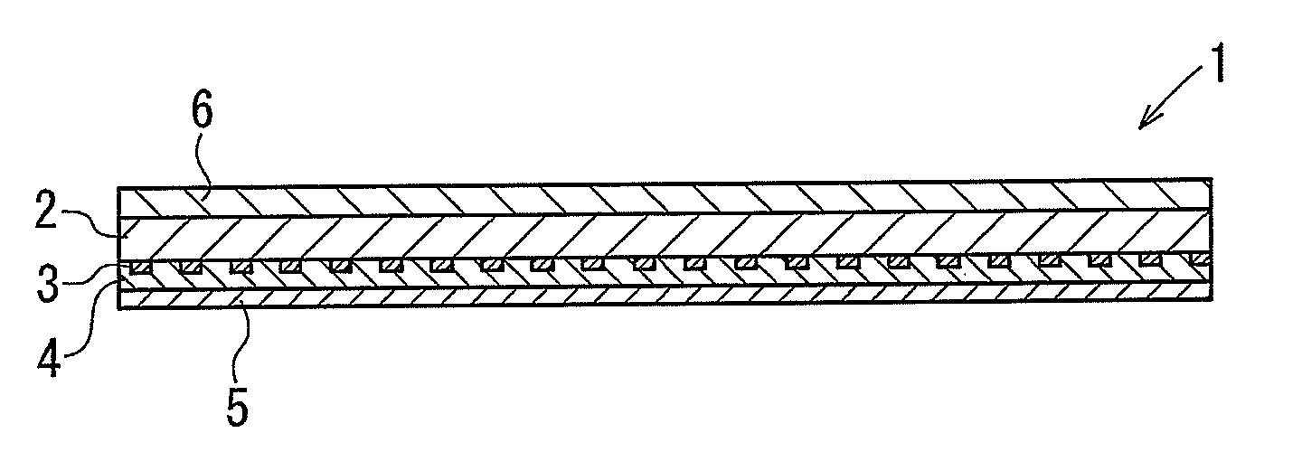
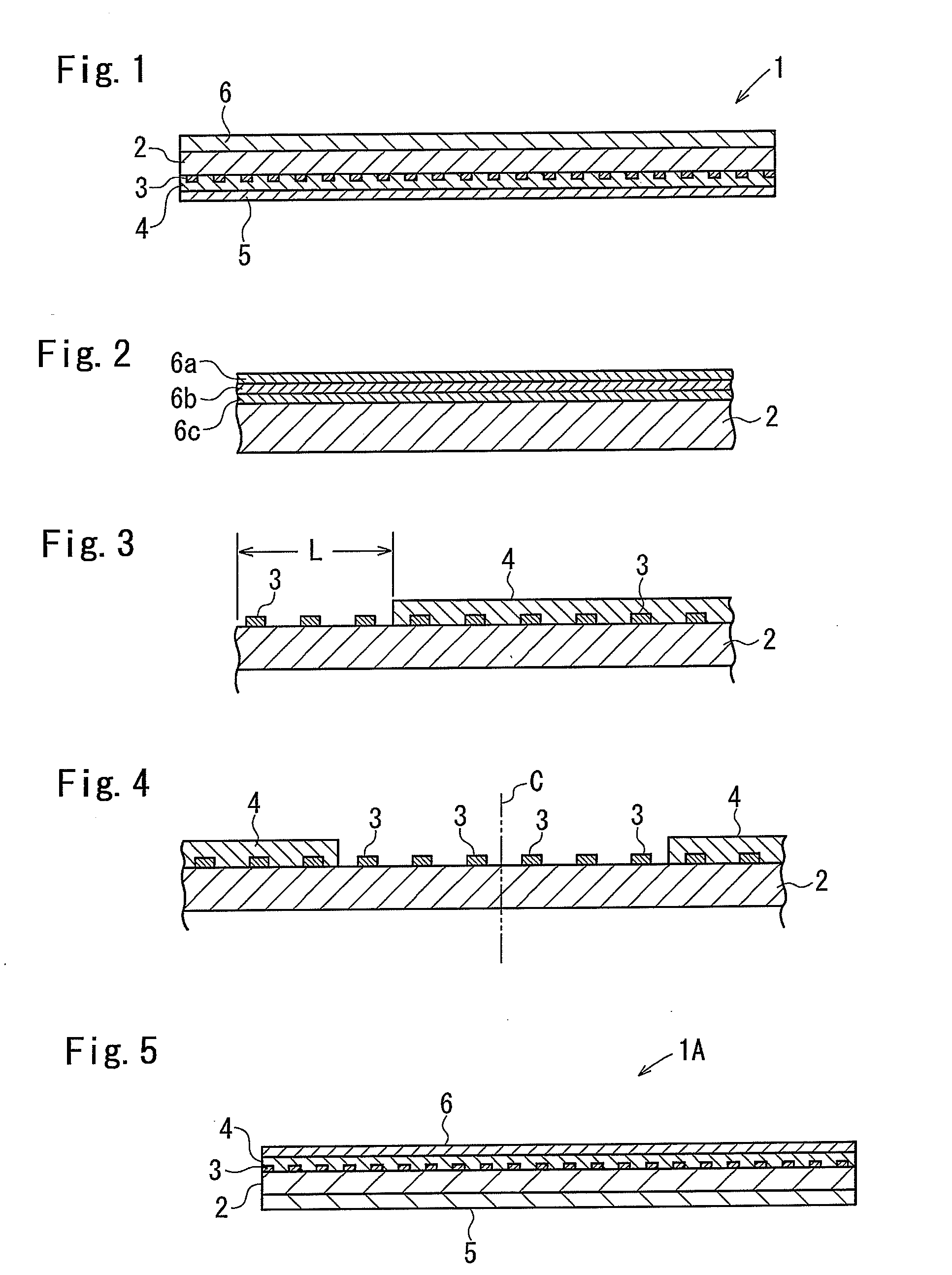
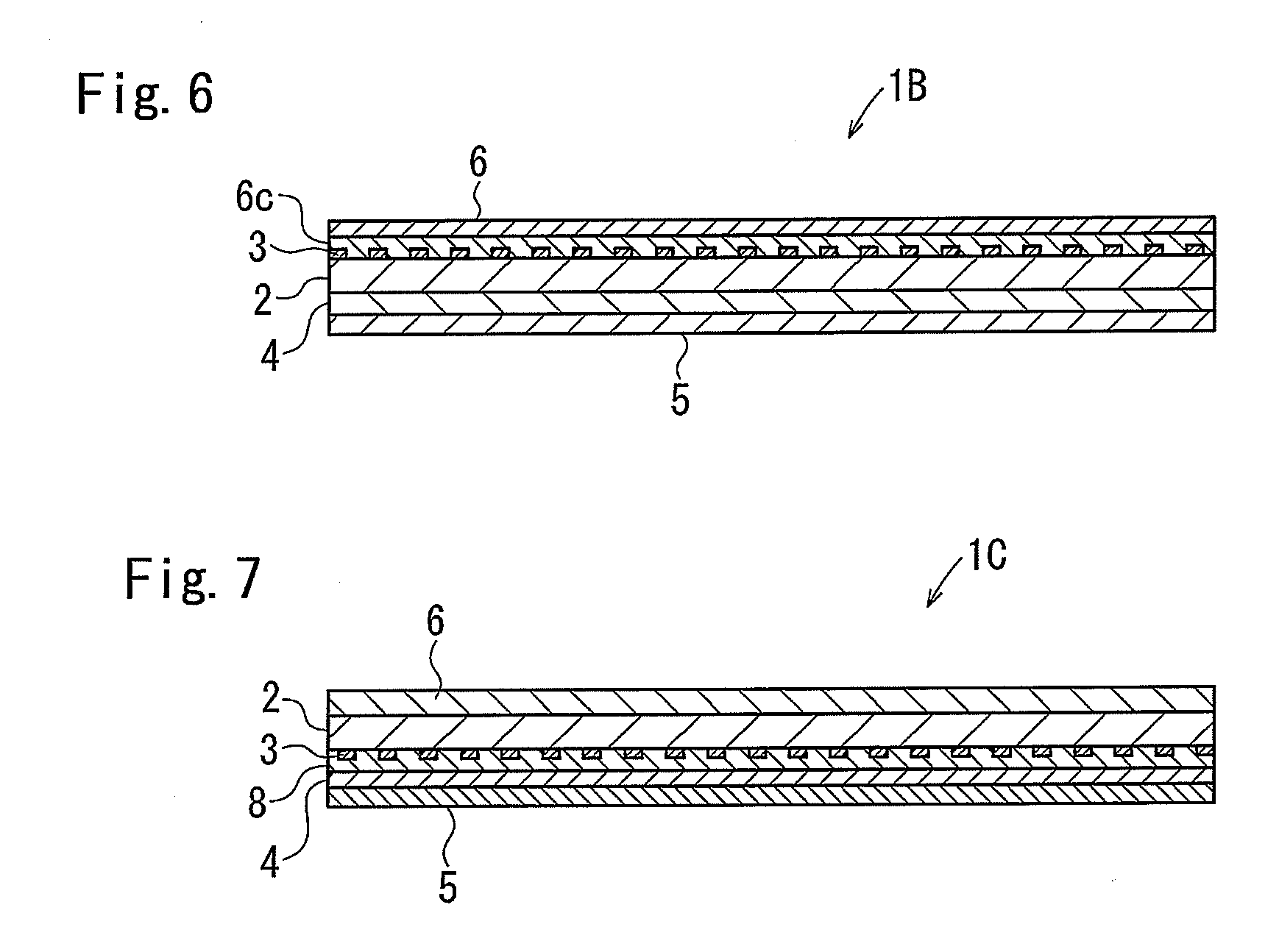
[0018]A display panel film 1 shown in FIG. 1 includes a base film 2, a conductive mesh 3 as a conductive layer disposed on one of the surfaces of the base film 2, a near-infrared absorption layer 4 (hereinafter may be referred to as “absorption layer 4”) disposed on the surface of the base film and covering the conductive mesh 3, an adhesive layer 5 disposed on the absorption layer 4, and an antireflection layer 6 disposed on the other surface of the base film 2.

[0019]The display panel film 1 using only one base film 2 is small in thickness.

[0020]As examples of the base film 2 include transparent films such as polyester, polyethylene terephthalate (PET), polybutylene terephthalate, polymethyl methacrylate (PMMA), acrylic, polycarbonate (PC), polystylene, cellulose triacet...


PUM

PropertyMeasurementUnit
thickness T2aaaaaaaaaa
thicknessaaaaaaaaaa
thicknessaaaaaaaaaa

Abstract

A multifunctional thin display panel film 1 includes a base film 2, a conductive mesh 3 disposed on a surface of the base film 2, an absorption layer 4 covering the conductive mesh 3 and being disposed on the surface of the base film 2 to absorb neon-emission light and infrared light, an adhesive layer 5 disposed on the near-infrared absorption layer 4, and an antireflection layer 6 disposed on the other surface of the base film 2.

Description

CROSS REFERENCE TO RELATED APPLICATION[0001]This is a continuation application of PCT / JP2006 / 309660 filed on May 15, 2006.FIELD OF THE INVENTION[0002]The present invention relates to display panels such as a plasma display panel (PDP) and to display panel films attached on the front surface of display panels.BACKGROUND OF THE INVENTION[0003]As a front filter for a PDP or the like, a laminated filter composed of a near-infrared cut film having a near-infrared absorption layer disposed on a base film, an antireflection film having an antireflection layer disposed on a base film, and a conductive mesh held between the near-infrared cut film and the antireflection film, the conductive mesh acting as an electromagnetic wave shield is described in paragraph [0050] of Japanese Unexamined Patent Application Publication No. 2001-320193.Patent Document 1: Japanese Unexamined Patent Application Publication No. 2001-320193[0004]As described in Japanese Unexamined Patent Application Publication ...

Claims


Application Information

Patent Timeline
Patent Type & Authority Applications(United States)
IPC IPC(8): F21V11/00H01J5/16
CPCB32B5/02B32B7/12B32B7/02
Inventor SUGIMACHI, MASATOISHII, YORINOBU
Owner BRIDGESTONE CORP
Why Eureka
Try Eureka