Structure for Functional Film Pattern Formation and Method of Manufacturing Functional Film

Inactive Publication Date: 2008-06-12
FUJIFILM CORP
View PDF10 Cites 9 Cited by
  • Summary
  • Abstract
  • Description
  • Claims
  • Application Information

AI Technical Summary

Benefits of technology

[0012]According to the present invention, the functional film is formed on the substrate in which the pattern has been formed in advance, and thereby, the process of performing dry etching or wet etching on the functional film can be omitted. Although sometimes damage is caused to the functional film in the etching step depending on the material, such damage is not caused according to the present invention. Further, the functional film is formed on the substrate via the separation layer, and therefore, by applying heat, an electromagnetic wave or an external force to the layer to be peel

Problems solved by technology

However, it is known that the functional film formed by film formation does not sufficiently exert its function in a condition after the film formation, and the film is inferior to a bulk material in performance.
However,

Method used


Image

  • Structure for Functional Film Pattern Formation and Method of Manufacturing Functional Film
  • Structure for Functional Film Pattern Formation and Method of Manufacturing Functional Film
  • Structure for Functional Film Pattern Formation and Method of Manufacturing Functional Film

Examples


example 1

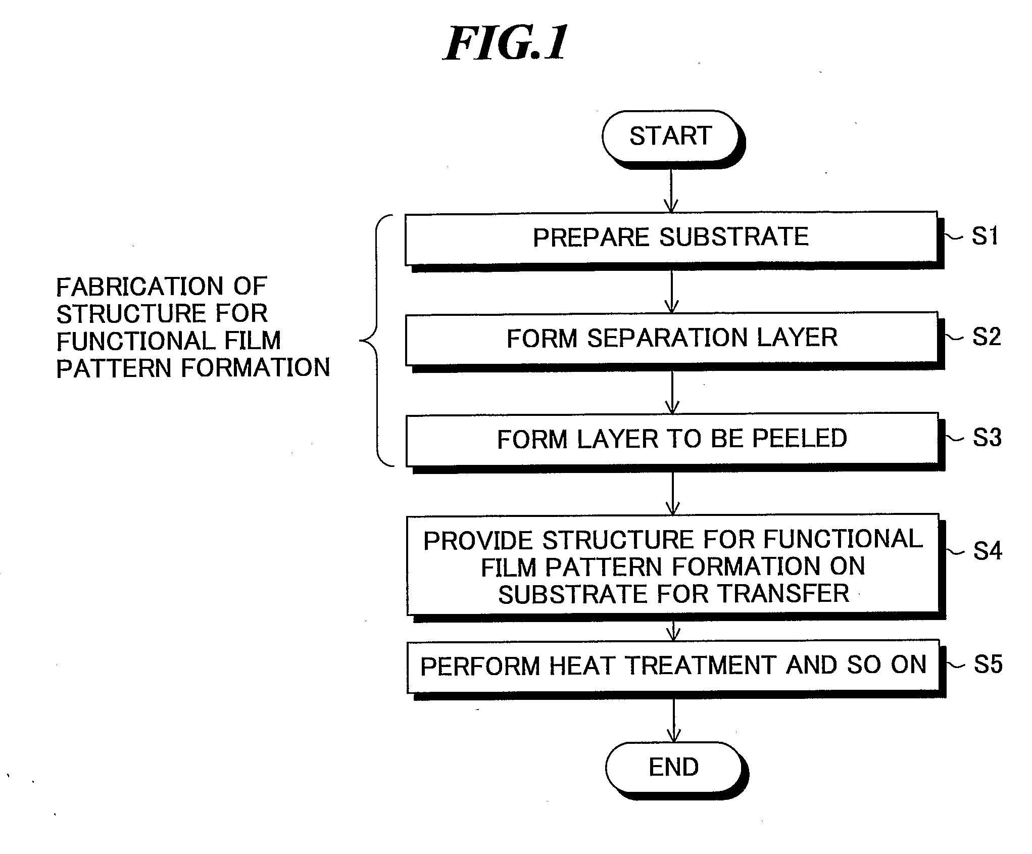
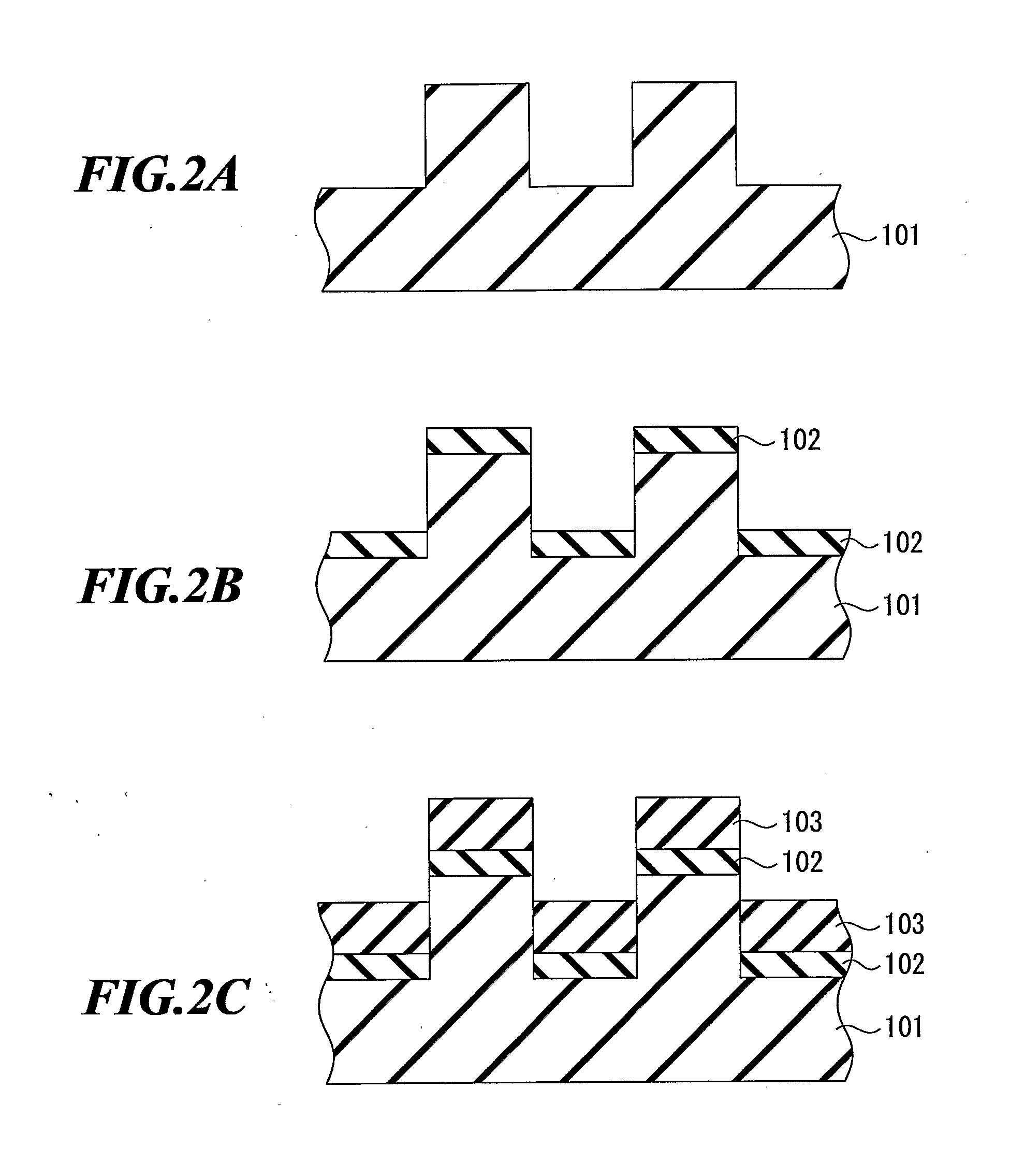
[0061]First, a quartz mold is fabricated. For the purpose, a resist is applied to a quartz substrate, and exposure to light and development are performed, and thereby, a resist pattern is formed. Then, a pattern is formed on the quartz substrate by dry etching by using the resist pattern as a mask. Furthermore, ashing (resist peeling) is performed.

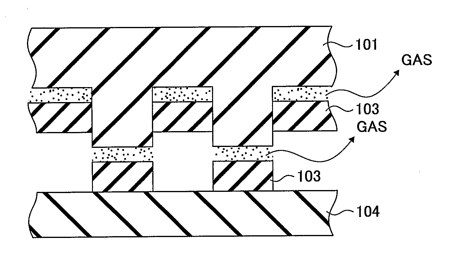
[0062]On the thus fabricated quartz mold, a tantalum nitride (TaN) film having a thickness of about 0.1 μm is formed as a separation layer by using a PLD (pulse laser deposition) method. A lower electrode of platinum (Pt) is formed on the tantalum nitride film by using the sputtering method, and a BST (barium strontium titanate) film having a thickness of about 200 nm is formed thereon by using the PLD method. At this time, the substrate temperature is heated to about 550° C. Furthermore, an upper electrode of platinum is formed on the BST film by using the sputtering method, and thereby, a Pt / BST / Pt thin film capacitor is fabricated.

[0063...

example 2

[0077]First, a quartz mold is fabricated. For the purpose, a resist is applied to a quartz substrate, and a resist pattern is formed by performing exposure to light and development. Then, a pattern is formed on the quartz substrate by dry etching by using the resist pattern as a mask. Furthermore, ashing (resist peeling) is performed.

[0078]On the thus fabricated quartz mold, a hexagonal boron nitride (h-BN) film having a thickness of about 0.2 μm is formed as a separation layer by using a reactive sputtering method. A lower electrode of platinum (Pt) is formed on the hexagonal boron nitride film by using the sputtering method, and a BST (barium strontium titanate) film having a thickness of about 200 nm is formed thereon by using the PLD method. At this time, the substrate is heated to a temperature of about 550° C. Furthermore, an upper electrode of platinum is formed on the BST film by using the sputtering method, and thereby, a Pt / BST / Pt thin film capacitor is fabricated.

[0079]Th...


PUM


Abstract

A method of manufacturing a functional film which method enables formation of a fine pattern and endurance for a high-temperature process. The method includes the steps of: (a) preparing a substrate in which a predetermined pattern is formed; (b) forming a separation layer directly or indirectly on the substrate; (c) forming a layer to be peeled containing a functional film, which is formed by using a functional material, on the separation layer; and (d) peeling the layer to be peeled from the substrate or reducing bonding strength between the layer to be peeled and the substrate by heating the separation layer, applying an electromagnetic wave toward the separation layer, or applying an external force to the separation layer.

Description


Claims


Application Information

Patent Timeline
Owner FUJIFILM CORP
Why Eureka
Try Eureka