Substrate treatment device

a treatment device and substrate technology, applied in the direction of polycrystalline material growth, crystal growth process, chemically reactive gas, etc., can solve the problems of inconvenient etching gas consumption and particle generation, and achieve good etching characteristics and avoid particle generation

Inactive Publication Date: 2008-06-12
KOKUSA ELECTRIC CO LTD
View PDF4 Cites 119 Cited by
  • Summary
  • Abstract
  • Description
  • Claims
  • Application Information

AI Technical Summary

Benefits of technology

[0011]According to this invention, since it is possible to adjust both of a growth speed and an etc

Problems solved by technology

Also, when the raw material gas and the etching gas are supplied from an identical nozzle, a film that is formed due to self-decomposition of the raw materia

Method used


Image

  • Substrate treatment device
  • Substrate treatment device
  • Substrate treatment device

Examples


Embodiment Construction

[0015]One embodiment of this invention will be described below based on the drawings.

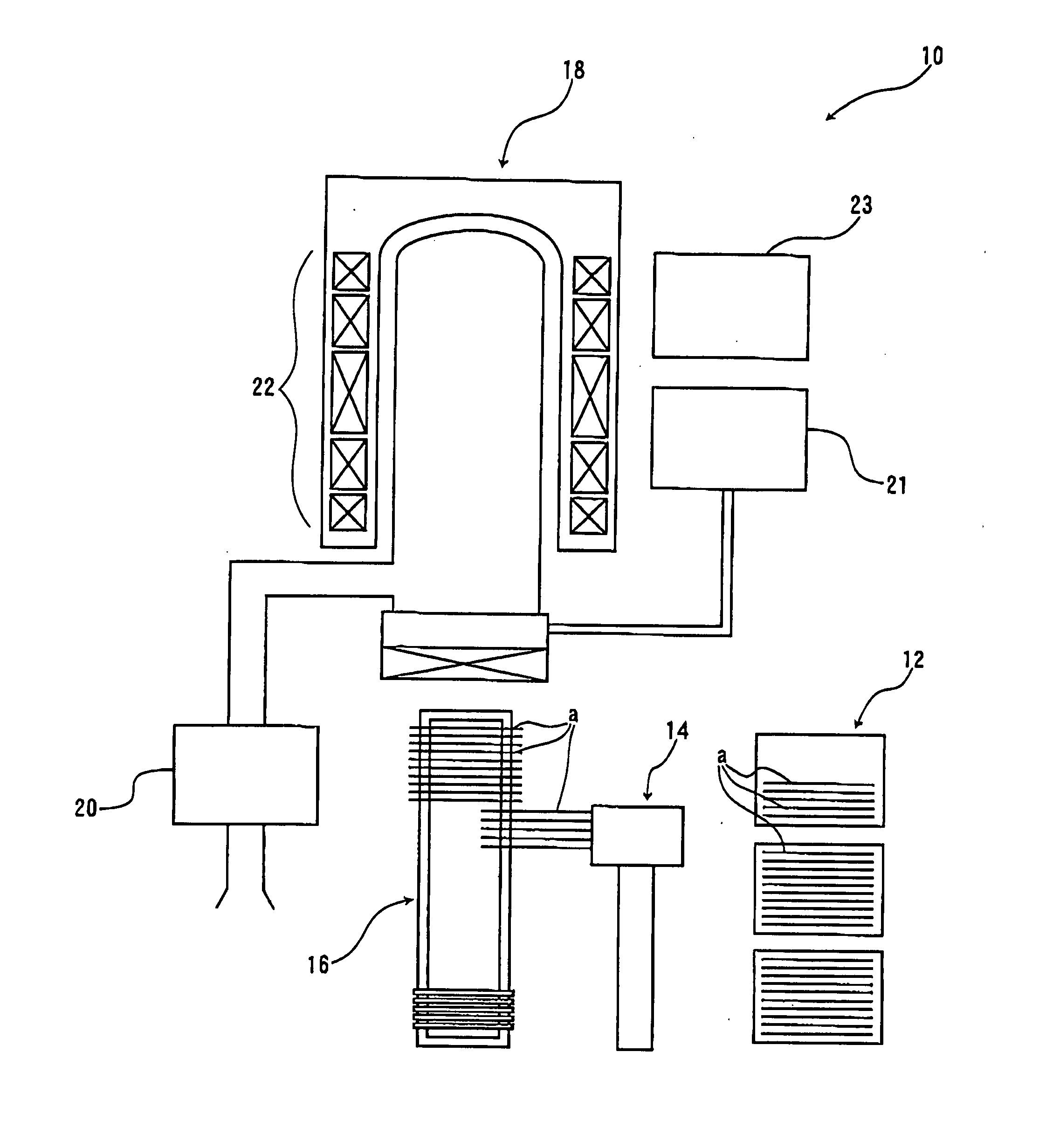
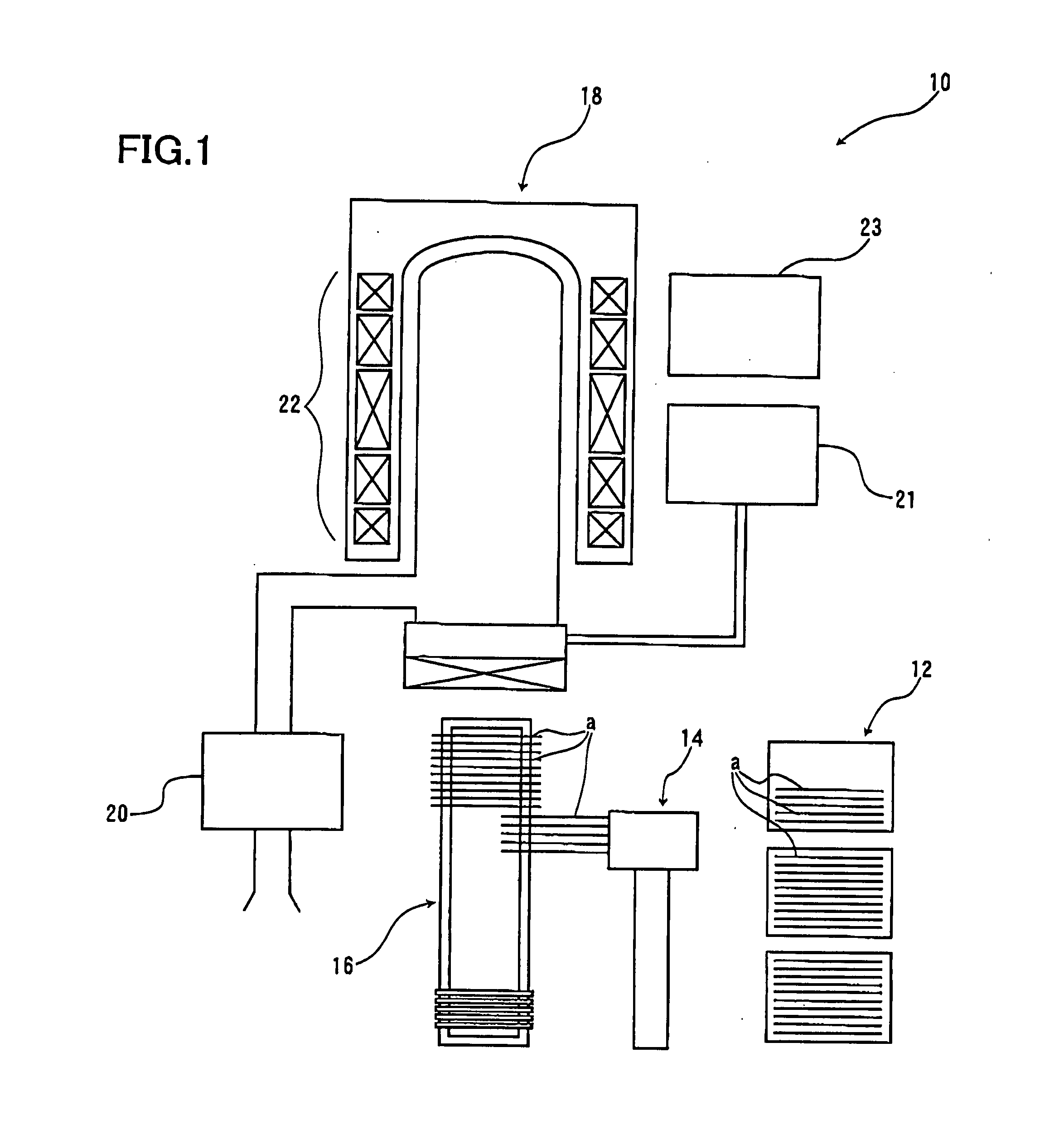
[0016]Shown in FIG. 1 is a schematic diagram of a substrate treatment device 10 according to one embodiment of this invention. The substrate treatment device 10 is a so-called hot wall type vertical low pressure CVD device.

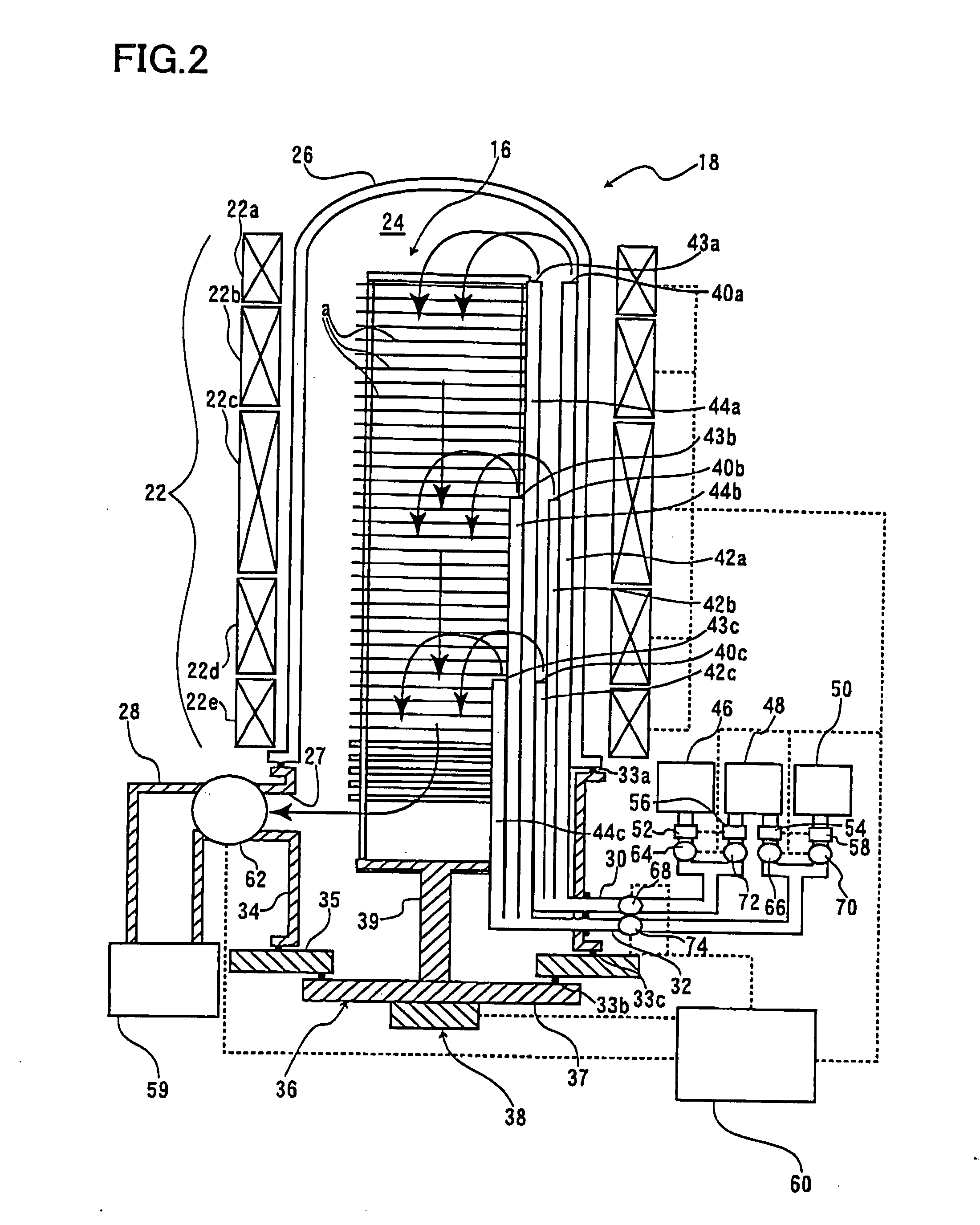
[0017]As shown in FIG. 1, wafers (Si substrates) a conveyed by a wafer cassette 12 are transferred onto a boat 16 from the wafer cassette 12 by a transfer machine 14. When transfer of all of the wafers a is finished, the boat 16 is inserted into a treatment furnace 18, and then the treatment furnace 18 is reduced in pressure by an evacuation system 20. Subsequently, a temperature inside the treatment furnace 18 is increased to a desired temperature by a heater 22, and, when the temperature becomes stable, a raw material gas and an etching gas are alternately supplied from a gas supply system 21 to cause selective epitaxial growth of Si, SiGe, or the like on the wafers a. Denoted b...


PUM

PropertyMeasurementUnit
Heightaaaaaaaaaa

Abstract

It is intended to provide a substrate treatment device capable of adjusting both of a growth speed and an etching speed in a selective epitaxial growth, avoiding particle generation from nozzles, and achieving good etching characteristics. A substrate treatment device for selectively growing an epitaxial film on a surface of a substrate by alternately supplying a raw material gas containing silicon and an etching gas to a treatment chamber, the substrate treatment device being provided with a substrate support member for supporting the substrate in the treatment chamber, a heating member provided outside the treatment chamber for heating the substrate and an atmosphere of the treatment chamber, a gas supply system provided inside the treatment chamber, and a discharge port opened on the treatment chamber, wherein the gas supply system comprises first gas supply nozzles for supplying the raw material gas and second gas supply nozzles for supplying the etching gas.

Description

BACKGROUND OF THE INVENTION[0001]1. Field of the Invention[0002]This invention relates to a substrate treatment device to be used for a semiconductor production apparatus.[0003]2. Description of the Related Art[0004]A reaction furnace (treatment furnace) of a vertical low pressure CVD device used for selective epitaxial growth of Si or SiGe is formed of a reaction piping, an inlet flange, a seal cap, and the like, wherein a boat is placed on the seal cap, a wafer is placed on the boat, and the reaction furnace is heated by a heater.[0005]In the above-mentioned structure, a gas serving as a raw material for the Si or SiGe selective epitaxial growth is introduced from an upper part of the reaction furnace through a nozzle and discharged from a lower part. Accordingly, in a reaction atmosphere where the wafer is present, the gas flows from the top to the bottom.[0006]In this case, the heater heating the reaction furnace is divided into five regions of an upper heater, a central upper h...

Claims


Application Information

Patent Timeline
IPC IPC(8): B44C1/22C23C16/00
CPCC23C16/22C23C16/24C30B35/00C30B25/14C30B29/06C30B25/08
Inventor YOKOGAWA, TAKASHIINOKUCHI, YASUHIROYAMAMOTO, KATSUHIKOHASHIBA, YOSHIAKIOGAWA, YASUHIRO
Owner KOKUSA ELECTRIC CO LTD
Why Eureka
Try Eureka