Single Chip Having Magnetoresistive Memory

a single chip and magnetoresistive technology, applied in the field of single chips, can solve the problems of low yield, low total number of soc chips per wafer, and high cost of soc chips, and achieve the effects of increasing memory size, reducing chip size, and simplifying manufacturing process

Inactive Publication Date: 2008-06-12
NORTHERN LIGHTS SEMICON
View PDF19 Cites 22 Cited by
  • Summary
  • Abstract
  • Description
  • Claims
  • Application Information

AI Technical Summary

Benefits of technology

[0008]It is another aspect of the present invention to provide a single chip having a magnetoresistive memory, in which a magnetoresistive memory layer is on a substrate having logic circuits. The single chip simplifies the manufacturing process, decreases chip size and increases memory size, thus reducing the manufacturing cost.

Problems solved by technology

Moreover, the embedded memories 104 are typically laid out adjacent to the logic circuits 102, and thus consume precious silicon area.
Thus, the conventional SOC chip leads to a very low yield, a low total number of SOC chips per wafer, and therefore high costs.

Method used


Image

  • Single Chip Having Magnetoresistive Memory
  • Single Chip Having Magnetoresistive Memory
  • Single Chip Having Magnetoresistive Memory

Examples


Embodiment Construction

[0018]Reference will now be made in detail to the present preferred embodiments of the invention, examples of which are illustrated in the accompanying drawings. Wherever possible, the same reference numbers are used in the drawings and the description to refer to the same or like parts.

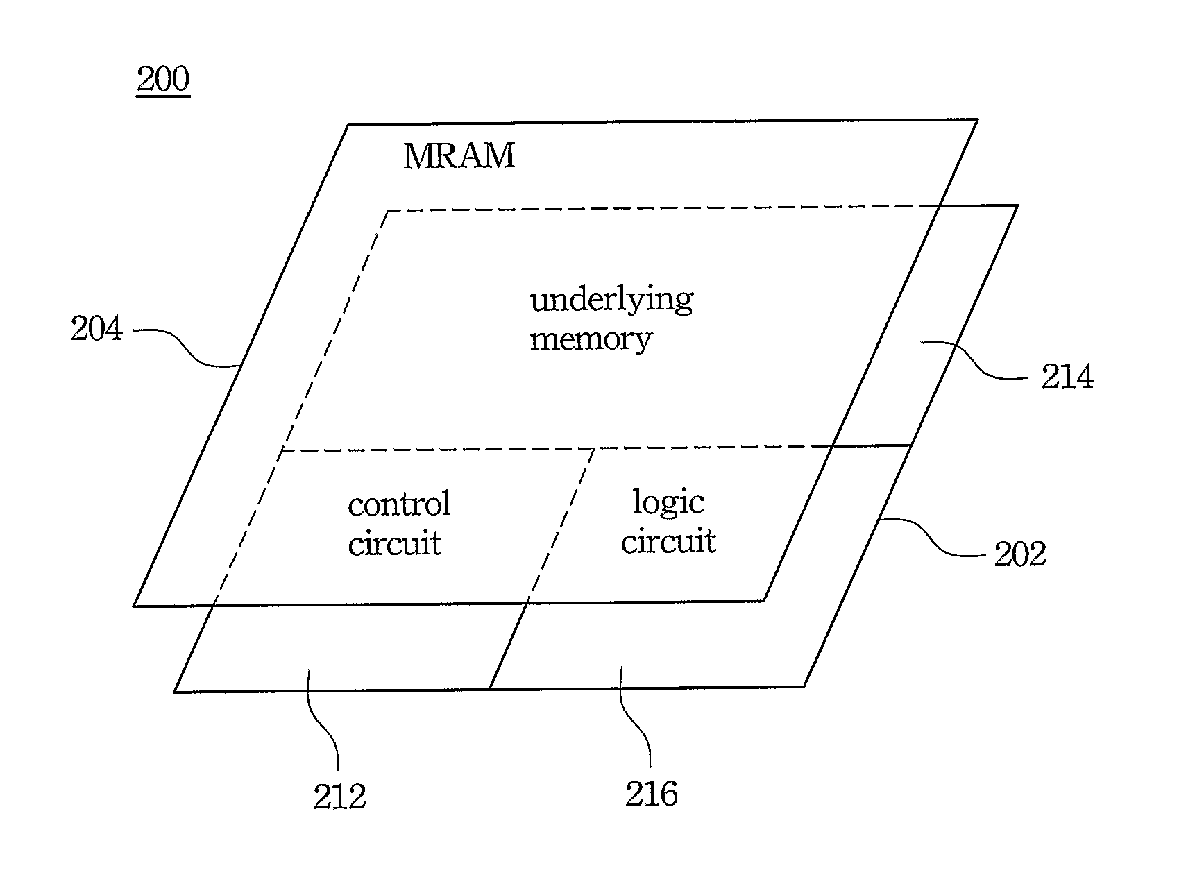
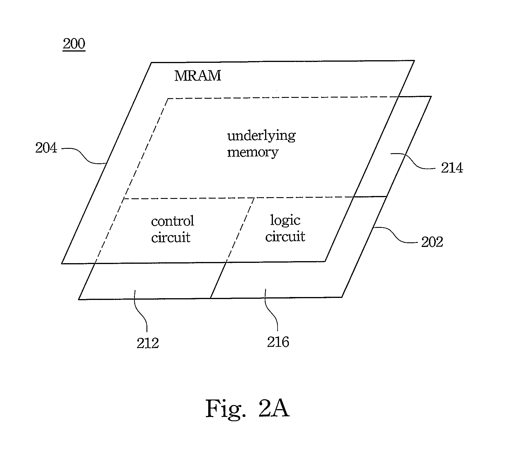
[0019]Magnetoresistive random access memory (MRAM) is a type of non-volatile memory with fast programming time and high density. The MRAM architecture includes a plurality of MRAM, cells and intersections of word lines and bit lines. A MRAM cell includes two ferromagnetic layers separated by a non-magnetic layer. Information is stored as directions of magnetization vectors in the two ferromagnetic layers.

[0020]The resistance of the non-magnetic layer between the two ferromagnetic layers indicates a minimum value when the magnetization vectors of the two ferromagnetic layers point in substantially the same direction. On the other hand, the resistance of the non-magnetic layer between the two ferromagn...


PUM


Abstract

A single chip has a substrate and at least one magnetoresistive memory layer. The substrate has an underlying memory and a control circuit. The magnetoresistive memory layer is placed on the substrate, and has a plurality of magnetoresistive random access memory cells controlled by the control circuit.

Description

BACKGROUND[0001]1. Field of Invention[0002]The present invention relates to a single chip. More particularly, the present invention relates to a single chip having magnetoresistive memory.[0003]2. Description of Related Art[0004]System-on-chip (SOC) products are widely used with the developments of semiconductor techniques. An SOC generally has logic circuits and an embedded non-volatile memory, such as EPROM, EEPROM, FLASH memory or FeROM. FIG. 1 is a schematic view of a conventional SOC chip. As illustrated in FIG. 1, a SOC chip 100 has logic circuits 102 and embedded memories 104. The logic circuits 102 include a microprocessor 112 and a control circuit 122 for memories. In the SOC chip 100, the embedded memories 104 are placed in the same plane as the logic circuits, and may have more than one type for different functions. For example, the embedded memories 104 may include a ROM 114, a RAM 124 and a FLASH memory 134.[0005]Generally, the logic circuits 102 sit on a p-substrate, a...

Claims


Application Information

Patent Timeline
Patent Type & Authority Applications(United States)
IPC IPC(8): G11C11/00G11C11/14
CPCG11C11/15G11C5/025
Inventor CHAN, CHIEN-CHIANGLAI, JAMES CHYI
Owner NORTHERN LIGHTS SEMICON
Why Eureka
Try Eureka