
Solid-state imaging element, photo-detector and authentication system using the photo-detector

a technology of solid-state imaging and authentication system, which is applied in the field photodetector and authentication system using the photodetector, can solve the problems of insufficient improvement in detection sensitivity, and conventional methods have limitations in obtaining higher sensitivity, so as to improve detection efficiency for visible light or near-infrared light, the detection sensitivity of solid-state imaging element can be improved, and the cross-talk between pixels can

Inactive Publication Date: 2008-06-19
HITACHI LTD
View PDF4 Cites 33 Cited by
  • Summary
  • Abstract
  • Description
  • Claims
  • Application Information

AI Technical Summary

Benefits of technology

[0013]The present invention solves the aforementioned problem by employing, in a solid-state imaging element, a structure where reflecting layers are provided on both sides of a photoelectric conversion means, and light (photons) is efficiently entered into the photoelectric conversion means, and further employing a structure where light (photons) that entered between the two reflecting layers does not flow outside.
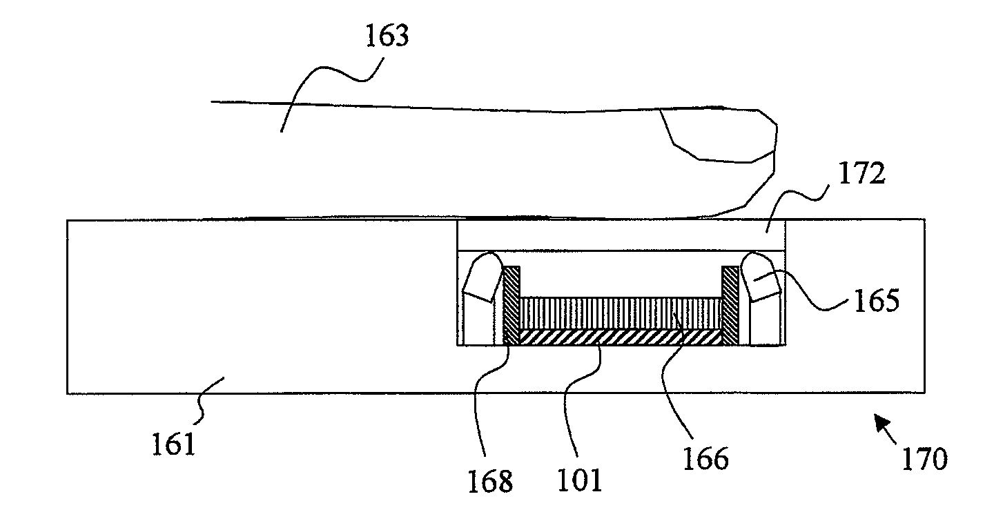
[0032]According to the present invention, detection sensitivity of a solid-state imaging element in which the photoelectric conversion film is manufactured with, for example, polysilicon or amorphous silicon can be improved. Moreover, in a photo-detector provided with a plurality of the solid-state imaging elements, detection efficiency for visible light or near-infrared light can be improved, and cross-talk between pixels can be reduced, which becomes more serious when higher sensitivity is desired. Furthermore, a highly precise personal authentication system comprising the solid-state imaging elements or the photo-detector can be provided.

Problems solved by technology

However, with the structures of Patent documents 1 and 2 mentioned above, there is a case where the improvement in detection sensitivity cannot be considered sufficient.
Moreover, by the method described in Patent document 3, multiple scattering can be caused only for a small part of photons in the photoelectric conversion film, and there is a case where the improvement in detection sensitivity cannot be considered sufficient.
As described above, the conventional methods have a limitation in obtaining higher sensitivity.

Method used


Image

  • Solid-state imaging element, photo-detector and authentication system using the photo-detector
  • Solid-state imaging element, photo-detector and authentication system using the photo-detector
  • Solid-state imaging element, photo-detector and authentication system using the photo-detector

Examples


first embodiment

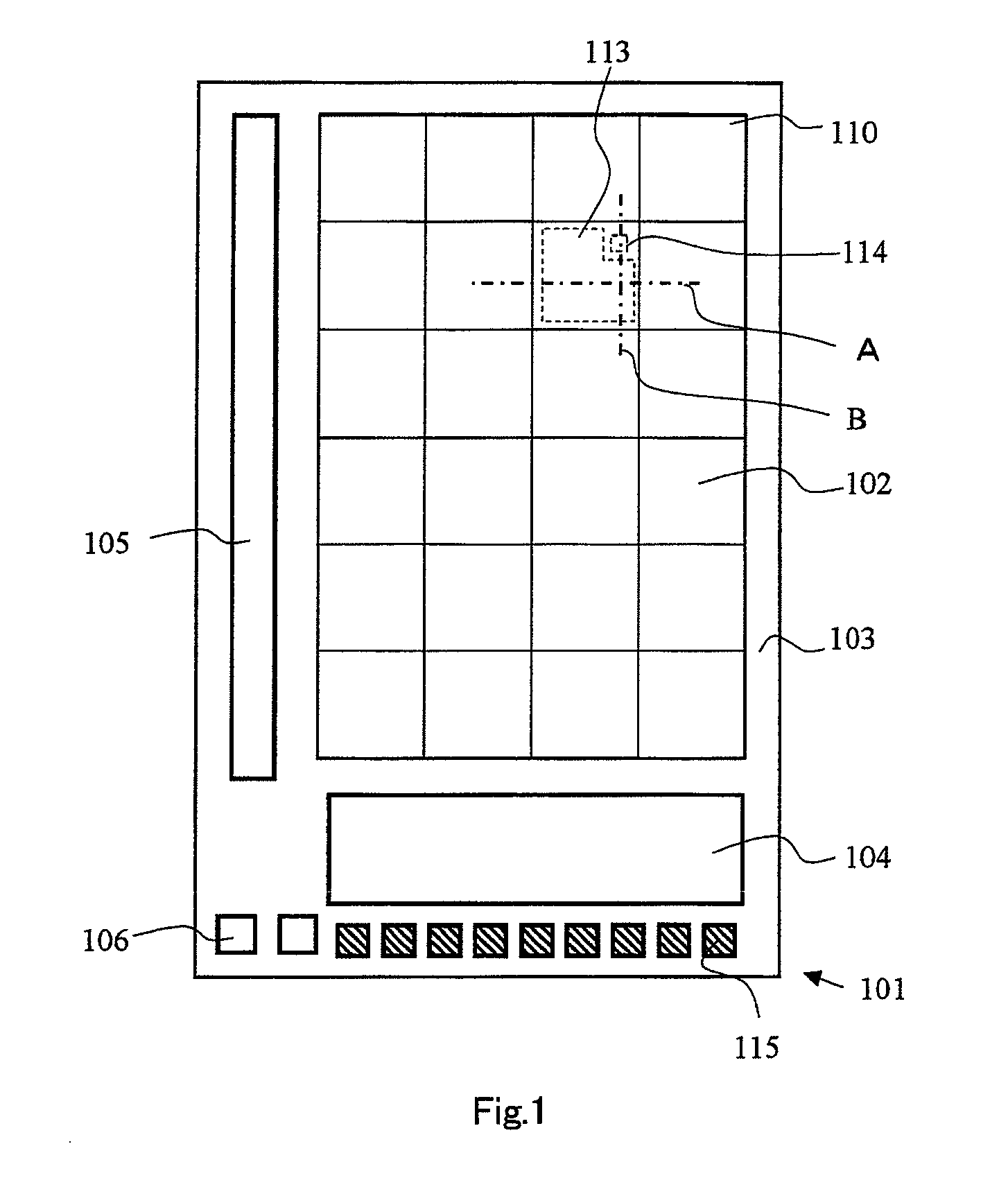
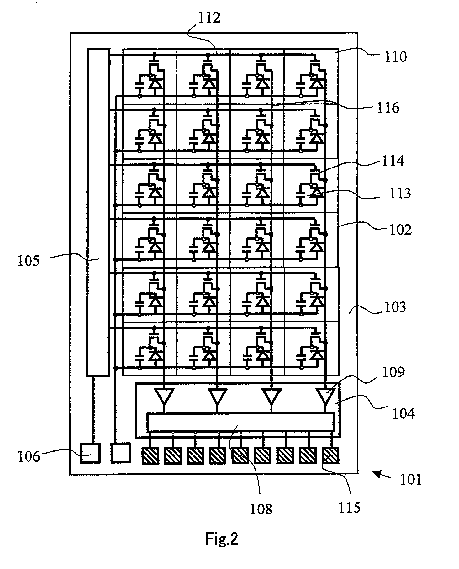
[0061]The structure of the solid-state imaging element 110 of the present invention according to the first embodiment is shown in FIG. 3. FIG. 3 shows a sectional view of the solid-state imaging element shown in FIG. 1 along the sectional line A. In the drawing, the upper side is the side for receiving incident photons 132, and width 126 is the width of one solid-state imaging element 110. This solid-state imaging element 110 has a structure where a reflecting layer (second reflecting layer) 120, a transparent layer 136, a photoelectric conversion element 135, a reflecting layer (first reflecting layer) 121 and a microlens 122 are formed on a substrate 103, the second reflecting layer 120 and the first reflecting layer 121 sandwich the adjacent transparent layer 136 and photoelectric conversion element 135, and further the microlens 122 is disposed on the first reflecting layer 121.

[0062]Further, in the example shown in FIG. 3, the reflecting layer 120 is adhered to the substrate 10...

second embodiment

[0093]The photo-detector of the present invention according to the second embodiment will be explained with reference to FIG. 7. In FIG. 7, the same elements as those of the first embodiment are indicated with the same symbols (the same shall apply to the following drawings).

[0094]In the photo-detector of this embodiment, the shape of the second reflecting layer 120 differs from that of the second reflecting layer 120 of the first embodiment. The other configurations are the same as those of the first embodiment. That is, the second reflecting layer 120 of this embodiment has a plurality of convexes and concaves on the reflecting surface as shown in FIG. 7. When it reflects the incident photons 132, it can thereby reflect them with a large amount of horizontal components, in other words, it can reflect them with a large reflection angle. This makes it possible to reflect photons which entered from the light entrance window 128 to the first reflecting layer 121, and therefore the amo...

third embodiment

[0103]The photo-detector of the present invention according to the third embodiment will explained below with reference to FIG. 8.

[0104]In the photo-detector of this embodiment, the shape of the second reflecting layer 120 differs from those of the first and second embodiments. The other configurations are the same as those of the first embodiment. That is, as shown in FIG. 8, the reflecting surface of the second reflecting layer 120 of this embodiment inclines. Incident photons are reflected by this reflecting surface to the first reflecting layer 121 on one side of the light entrance window 128.

[0105]Inclination of the reflecting surface for efficiently reflecting photons which entered from the light entrance window 128 to the first reflecting layer 121 will be explained. Here, in order to simplify the explanation, it is assumed that there shall be no refraction of light at the interfaces of the layers.

[0106]Also in this case, the inclination of the reflecting surface is designed ...


PUM


Abstract

In a solid-state imaging element, reflecting layers are provided on both sides of a photoelectric conversion means, a light entrance window 128 is provided in the first reflecting layer 121 disposed on the photon incidence side, and a concentration means 122 is provided at a position corresponding to the window. Further, a transparent layer 136 is provided between the photoelectric conversion means and a second reflecting layer 120. A structure where photons that entered between the two reflecting layers do not flow outside is preferably employed as the shape of the second reflecting layer 120. According to the present invention, detection sensitivity of a solid-state imaging element and a photo-detector using the same is improved, and a personal authentication system carrying a photo-detector showing improved detection sensitivity is provided.

Description

CLAIM OF PRIORITY[0001]The present application claims priority from Japanese application JP2006-338489 filed on Dec. 15, 2006, the content of which is hereby incorporated by reference into this application.BACKGROUND OF THE INVENTION[0002]1. Technical Field[0003]The present invention relates to a photoelectric conversion element formed with a thin film of a photoelectric absorption material such as polysilicon film or amorphous silicon film, a solid-state imaging element or detector such as image sensor, solar cell and X-ray flat panel sensor, and a system such as liquid crystal display, biometric personal authentication system, photovoltaic power generation system, X-ray imaging system and digital camera using the same.[0004]2. Background Art[0005]In photo-detectors for visible light, crystalline silicon has mainly been used so far to date. However, use of thin-film sensors using amorphous silicon or polysilicon is spreading in recent years.[0006]Amorphous silicon films are also us...

Claims


Application Information

Patent Timeline
IPC IPC(8): H01L27/00H01L31/00G06T1/00H01L27/14H01L27/146H04N1/028H04N5/335H04N5/369H04N5/3745
CPCH01L27/14623H01L27/14627H01L31/022466H01L27/14643H01L27/14678H01L27/14632
Inventor KONNO, YASUTAKAUEKI, HIRONORI
Owner HITACHI LTD
Learn More