Multi-gated carbon nanotube field effect transistor

Inactive Publication Date: 2008-06-26
MOTOROLA INC
View PDF8 Cites 9 Cited by
  • Summary
  • Abstract
  • Description
  • Claims
  • Application Information

AI Technical Summary

Benefits of technology

[0012]A multiple, independent top gated field effect transistor and a method that allows for the destruction of metallic carbon nanotubes positioned between the source and drain of a top multi-gate transistor are provided. The field effect transistor comprises at least one carbon nanotubes coupled between the first and second electrodes and a first gate material formed over a portion of the at least one carbon nanotubes

Problems solved by technology

In contrast with zero-dimensional, e.g., quantum dots, and two-dimensional nanostructures, e.g., GaAs/AlGaAs superlattice, direct synthesis and growth of one-dimensional nanostructures has been relatively slow due to difficulties associated with controlling the chemical composition, dimensions, and morphology.
This limits the range of usuable drain voltages and the achievable on currents.
However, stronger capacitive coupling between the gate and drain will reduce the barrier for minority carrier injection on the drain side (referred to as gate-induced-barrier-lowering (GIBL)) and result in inferior performance such as reduced ON/OFF current ratio and ambipolar transport.
While normalized transconductance of a single nanotube FET can be quite large, the overall transconductance is small due to the intrin

Method used


Image

  • Multi-gated carbon nanotube field effect transistor
  • Multi-gated carbon nanotube field effect transistor
  • Multi-gated carbon nanotube field effect transistor

Examples


Embodiment Construction

[0022]The following detailed description of the invention is merely exemplary in nature and is not intended to limit the invention or the application and uses of the invention. Furthermore, there is no intention to be bound by any theory presented in the preceding background of the invention or the following detailed description of the invention.

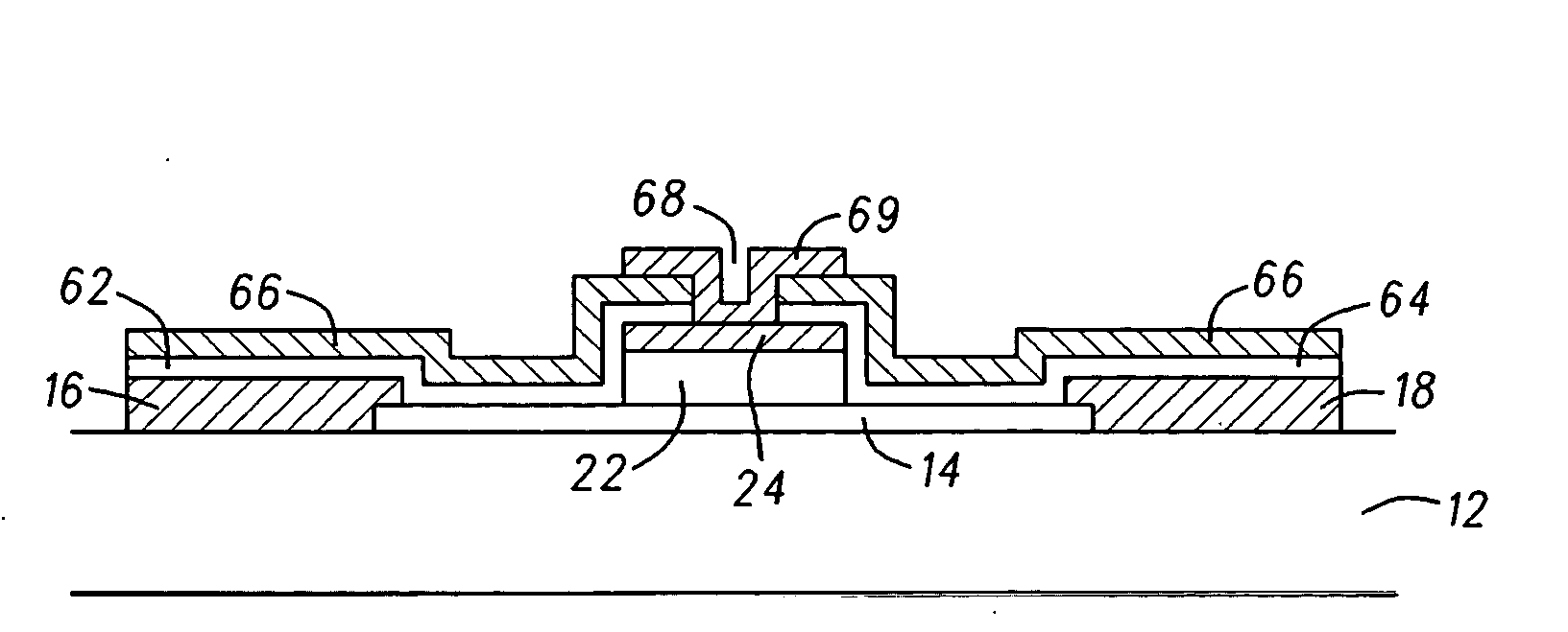
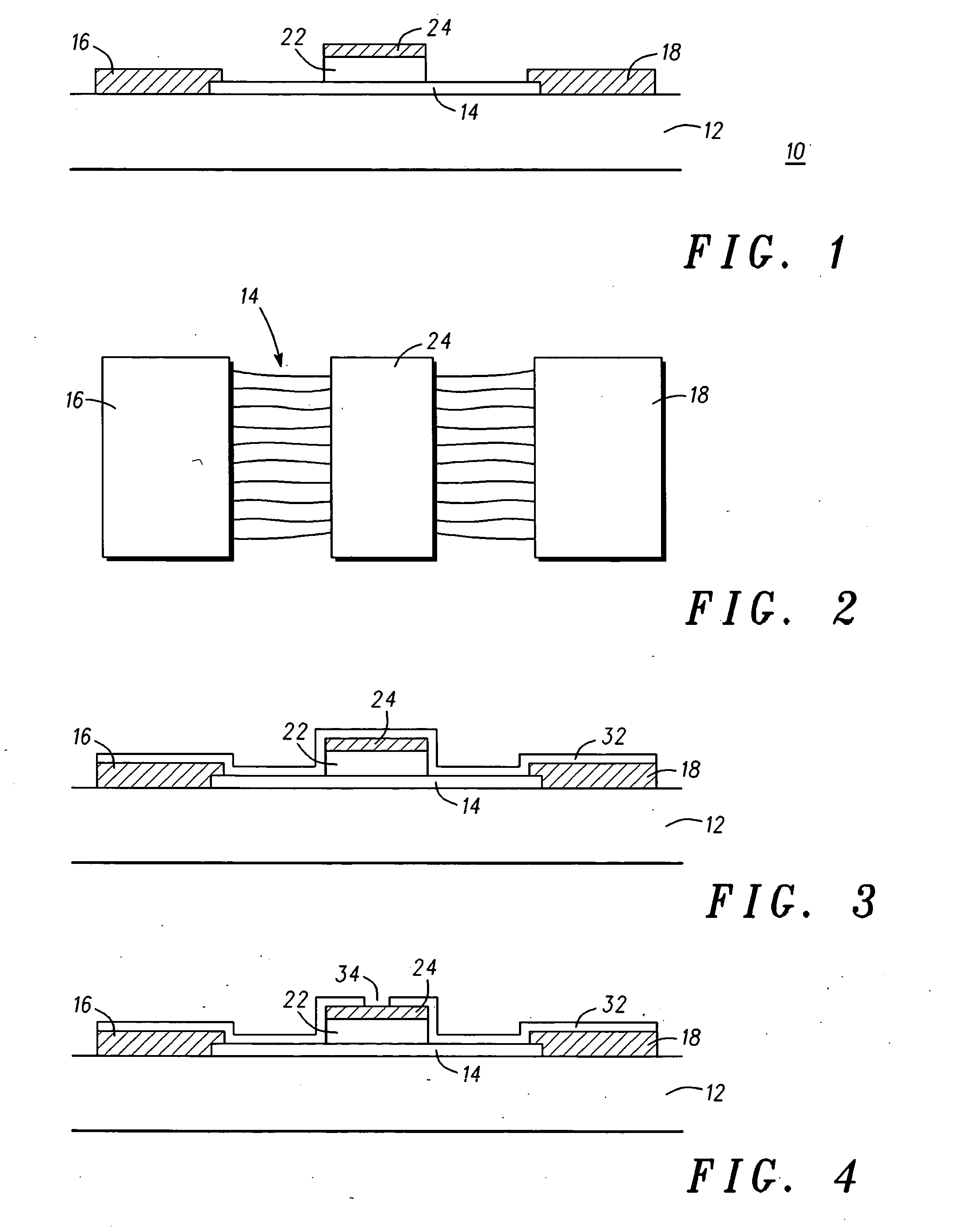
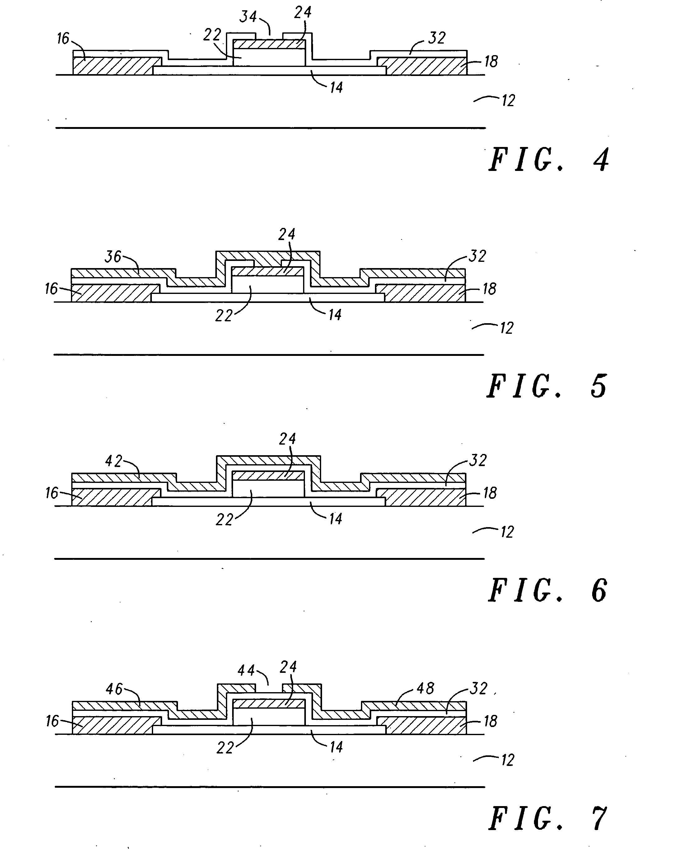
[0023]One-dimensional nanostructures such as nanotubes and nanowires show promise for the development of molecular-scale sensors, resonators, field emission displays, and logic / memory elements. One-dimensional nanostructures are herein defined as a material having a high aspect ratio of greater than 10 to 1 (length to diameter).

[0024]In accordance with an exemplary embodiment, an under lapped top-gated field effect transistor is formed with one-dimensional nanostructures as the channel between the source and drain. Optionally, an electrical burn-out of any metallic one-dimensional nanostructures is performed by applying a current between the...


PUM


Abstract

A multiple, independent top gated field effect transistor having an improved electron injection and reduced gate induced barrier lowering effects, and a method that allows for the destruction of metallic carbon nanotubes positioned between the source and drain of a top multi-gate transistor are provided. The field effect transistor comprises at least one carbon nanotube (14) coupled between the first and second electrodes (16, 18) and a first gate material (24) formed over a portion of the at least one carbon nanotube (14) and spaced apart from the first and second electrodes (16, 18). A dielectric material (32) is conformally coated on the first and second electrodes (16, 18), the at least one carbon nanotube (14), and the first gate material (24). A second gate material (36) is conformally coated on the dielectric material (32). Other exemplary embodiments include one gate (24, 36), three gates (24, 46, 48), and three gates (24, 54, 56; and 24, 66) having the dielectric layer (52, 56; and 62, 64) portioned with different material characteristics.

Description

FIELD OF THE INVENTION[0001]The present invention generally relates to field effect transistors and more particularly to a multiple, independent top gated field effect transistor having an improved electron injection and a method that allows for the destruction of metallic carbon nanotubes positioned between the source and drain of a top multi-gate transistor.BACKGROUND OF THE INVENTION[0002]One-dimensional nanostructures, such as belts, rods, tubes and wires, have become the focus of intensive research with their own unique applications. One-dimensional nanostructures are model systems to investigate the dependence of electrical and thermal transport or mechanical properties as a function of size reduction. In contrast with zero-dimensional, e.g., quantum dots, and two-dimensional nanostructures, e.g., GaAs / AlGaAs superlattice, direct synthesis and growth of one-dimensional nanostructures has been relatively slow due to difficulties associated with controlling the chemical composit...

Claims


Application Information

Patent Timeline
IPC IPC(8): H01L27/00H01L21/762
CPCB82Y10/00H01L51/0554H01L51/0048H10K85/221H10K10/482
Inventor THOMAS, SHAWN G.AMLANI, ISLAMSHAH S.
Owner MOTOROLA INC
Why Eureka
Try Eureka