Multiwavelength semiconductor laser array and method of fabricating the same

a multi-wavelength semiconductor and laser array technology, applied in the field of semiconductor lasers, can solve the problems of high cost of subsequent epitaxial regrowth and complicated fabrication process of the above multi-wavelength semiconductor lasers

Inactive Publication Date: 2008-06-26
IND TECH RES INST
View PDF6 Cites 27 Cited by
  • Summary
  • Abstract
  • Description
  • Claims
  • Application Information

AI Technical Summary

Benefits of technology

[0010]In view of the above problems, the present invention provides a multiwavelength semiconductor laser array and a method of fabricating the same, in which a laser array formed by a plurality of laser resonators is adopted with a simple fabrication process to change the lengths of resonant cavities or electrode layers on top of the laser resonators, such that each of the laser resonators generates a laser in a different wave band region.

Problems solved by technology

However, the fabrication process of the above multiwavelength semiconductor laser is very complicated, and the subsequent epitaxial regrowth has a rather high cost.

Method used


Image

  • Multiwavelength semiconductor laser array and method of fabricating the same
  • Multiwavelength semiconductor laser array and method of fabricating the same
  • Multiwavelength semiconductor laser array and method of fabricating the same

Examples


Embodiment Construction

[0028]The objectives, structures, features, and functions of the present invention will be illustrated in detail below accompanied with the embodiments. The above description of the content of the present invention and the following illustration of the embodiments are intended to demonstrate and explain the principles of the present invention and to provide further explanations of the claims of the present invention.

[0029](Structure of Multiwavelength Semiconductor Laser Array)

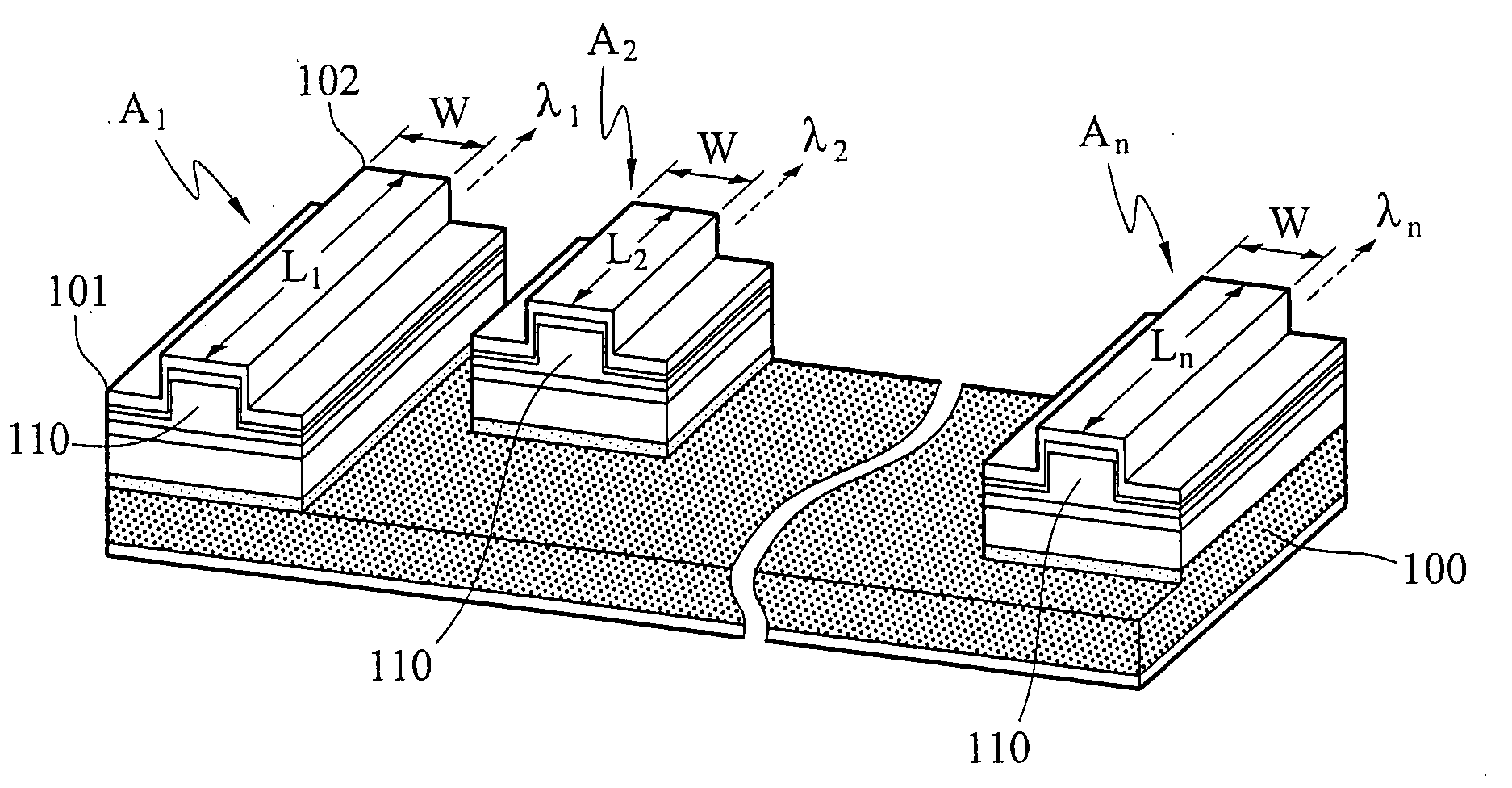
[0030]FIG. 1 is a structural stereogram of a multiwavelength semiconductor laser array according to a first embodiment of the present invention. As shown in FIG. 1, the. multiwavelength semiconductor laser array of the present invention includes a substrate 100 and N laser resonators A1 to An. The N laser resonators A1 to An are formed on the substrate 100, which are parallel to each other and each has a corresponding ridge waveguide structure 110. Each ridge waveguide structure 110 has a width of W. Moreover,...


PUM


Abstract

A multiwavelength semiconductor laser array and a method of fabricating the same are provided. Laser resonators having stacked quantum dot active regions of different emission wavelengths are utilized together with a fabricating process to change the length of each laser resonator or that of an upper electrode layer to generate different laser oscillation conditions, such that each of the laser resonators generates a single-wavelength band laser in a specific quantum dot active region, thereby achieving a multiwavelength semiconductor laser array capable of generating multiple laser wavelengths.

Description

CROSS-REFERENCE TO RELATED APPLICATIONS[0001]This non-provisional application claims priority under 35 U.S.C. §119(a) on Patent Application No(s). 095148051 filed in Taiwan, R.O.C. on Dec. 20, 2006, the entire contents of which are hereby incorporated by reference.BACKGROUND OF THE INVENTION[0002]1. Field of Invention[0003]The present invention relates to a semiconductor laser and a method of fabricating the same. More particularly, the present invention relates to a multiwavelength semiconductor laser array formed by a plurality of laser resonators and a method of fabricating the same.[0004]2. Related Art[0005]Recently, many research scholars have found that, compared with applications of semiconductor lasers such as bulk material without any quantum structure, quantum well, and quantum wire, the semiconductor laser having quantum dot as the active layer has an excellent laser property, and the quantum dot semiconductor laser is expected to have great potential in the application o...

Claims


Application Information

Patent Timeline
Patent Type & Authority Applications(United States)
IPC IPC(8): H01S5/40H01L21/00
CPCB82Y20/00H01S5/0425H01S5/1039H01S5/4087H01S5/22H01S5/3412H01S5/4031H01S5/16H01S5/1025
Inventor LIN, KUO-JUICHI, TUNG-WEILIN, KUN-FENGLAI, CHIH-MING
Owner IND TECH RES INST
Why Eureka
Try Eureka