Transistor, fabricating method thereof and flat panel display therewith

a technology of transistor and fabricating method, which is applied in the direction of basic electric elements, semiconductor devices, electrical apparatus, etc., can solve the problems of low electron mobility, long process time, and damage to silicon layers

Inactive Publication Date: 2008-07-03
SAMSUNG MOBILE DISPLAY CO LTD
View PDF8 Cites 25 Cited by
  • Summary
  • Abstract
  • Description
  • Claims
  • Application Information

AI Technical Summary

Benefits of technology

[0012]Aspects of the present invention are directed to controlling the concentration of the metal catalyst left in a polycrystalline silicon layer when an amorphous silicon layer formed on an insulating substrate is crystallized into a polycrystalline silicon layer using an SGS (Super Grain Silicon) crystallization method.

Problems solved by technology

However, if the amorphous silicon is deposited directly on a substrate by the chemical vapor deposition method and the like, the amorphous silicon layer containing about 12% of hydrogen is formed, which has low electron mobility.
In addition, if the amorphous silicon layer of low electron mobility is crystallized into a silicon layer with a crystalline structure having high electron mobility, the silicon layer can be damaged by an explosion of the hydrogen contained therein.
However, the solid phase crystallization has disadvantages in that the process time is too long, and the substrate can be deformed easily due to the high temperature heat treatment occurring over a long time.
The excimer laser crystallization has disadvantages in that the process requires an expensive laser device, and the interfacial property between a semiconductor layer and a gate insulating layer is poor because extrusions are generated on a polycrystallized surface.
The metal induced crystallization or the metal induced lateral crystallization have disadvantages in that a leak (or leakage) current of a semiconductor layer of a thin film transistor increases because metal catalysts are left in the polycrystalline silicon layer.
Consequently, the characteristics of various flat panel display devices using the silicon layer as a switching transistor or a driving transistor of the above processes are poor.

Method used


Image

  • Transistor, fabricating method thereof and flat panel display therewith
  • Transistor, fabricating method thereof and flat panel display therewith
  • Transistor, fabricating method thereof and flat panel display therewith

Examples


Embodiment Construction

[0029]Reference will now be made in detail to aspects of the present invention, examples of which are illustrated in the accompanying drawings, wherein like reference numerals refer to the like elements throughout. The aspects are described below in order to explain the present invention by referring to the figures.

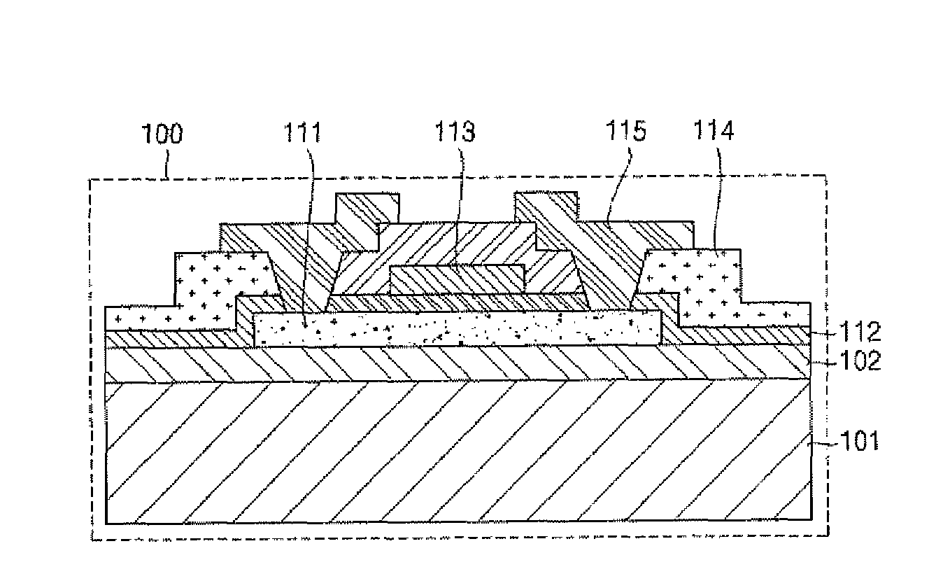
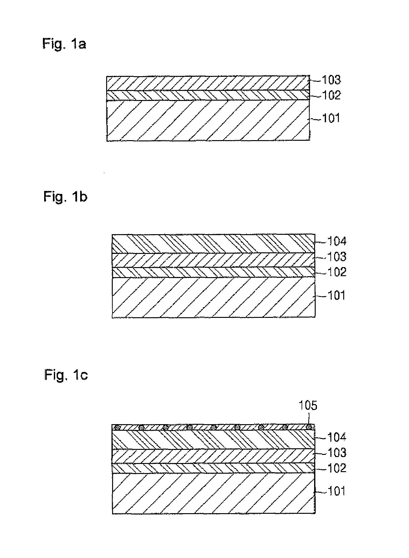
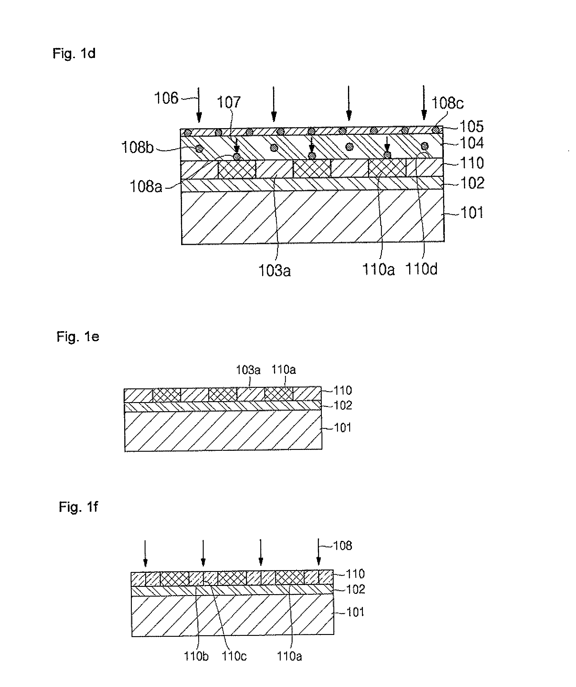
[0030]FIGS. 1A to 1F are cross-sectional views depicting a fabricating process wherein an amorphous silicon layer is crystallized into a polycrystalline silicon layer using an SGS (Super Grain Silicon) crystallization method according to an aspect the present invention. First, FIG. 1A is a cross-sectional view depicting a process during which a buffer layer 102 is formed on a substrate 101, and an amorphous silicon layer 103 is formed on the buffer layer 102. As shown in FIG. 1A, the buffer layer 102 is formed as a single layer or a double layer of a silicon oxide layer or a silicon nitride layer by use of a chemical vapor deposition technique or process or a physical vap...


PUM


Abstract

A transistor includes a substrate, an active region including a source region, a channel region, and a drain region which are crystallized using an SGS crystallization method and are formed on the substrate so that a grain size of a first annealed portion and a second annealed portion are different from each other, a gate insulating layer formed on the active region, and a gate electrode formed on the gate insulating layer.

Description

CROSS-REFERENCE TO RELATED APPLICATION[0001]This application claims the benefit of Korean Application No. 2006-138322 filed on Dec. 29, 2006, in the Korean Intellectual Property Office, the disclosure of which is incorporated herein by reference.BACKGROUND OF THE INVENTION[0002]1. Field of the Invention[0003]Aspects of the present invention relate to a transistor, a fabricating method thereof, and a flat panel display device therewith. More particularly, aspects of the present invention relate to a transistor, a fabricating method, and a flat panel display device, wherein an amorphous silicon layer formed on an insulating substrate is crystallized into a polycrystalline silicon layer using an SGS (Super Grain Silicon) crystallization method, whereby the substrate undergoes a first annealing process by absorbing or diffusing an extremely small amount of metal catalysts into a capping layer as the substrate undergoes a first heat treatment in order to control the concentration of the ...

Claims


Application Information

Patent Timeline
Patent Type & Authority Applications(United States)
IPC IPC(8): H01L29/04H01L21/00
CPCH01L21/02488H01L21/02532H01L21/02672H01L27/3244H01L27/1277H01L29/66757H01L29/78675H01L29/78696H01L29/04H10K59/12H01L27/1214
Inventor PARK, BYOUNGKEONYANG, TAEHOONSEO, JINWOOKJUNG, SEIHWANLEE, KIYONGLISACHENKO, MAXIM
Owner SAMSUNG MOBILE DISPLAY CO LTD
Why Eureka
Try Eureka