CMOS image sensor and fabricating method thereof

a technology of image sensor and fabrication method, which is applied in the direction of electrical equipment, semiconductor devices, radio frequency controlled devices, etc., can solve the problems of reducing the high power consumption of high-integrated systems, reducing the density required for high-integrated systems, and preventing leakage current, so as to prevent leakage current

Inactive Publication Date: 2008-07-03
DONGBU HITEK CO LTD
View PDF3 Cites 32 Cited by
  • Summary
  • Abstract
  • Description
  • Claims
  • Application Information

AI Technical Summary

Benefits of technology

[0015]An object of the present invention is to provide a method of fabricating a CMOS image sensor, in which a leakage current is prevented by performing a borderless contact forming process in

Problems solved by technology

The CCD image sensors have superior noise and photo sensitivity characteristics when compared to the CMOS image sensors, but have difficulties achieving the density required for highly integrated systems and reducing their high power consumption.
In one CMOS image sensor fabricating method currently used in the art, both salicidation and silicidation processes are simultaneously performed, making

Method used


Image

  • CMOS image sensor and fabricating method thereof
  • CMOS image sensor and fabricating method thereof
  • CMOS image sensor and fabricating method thereof

Examples


Embodiment Construction

[0024]Reference will now be made in detail to the preferred embodiments of the present invention, examples of which are illustrated in the accompanying drawings. Wherever possible, the same reference numbers will be used throughout the drawings to refer to the same or like parts.

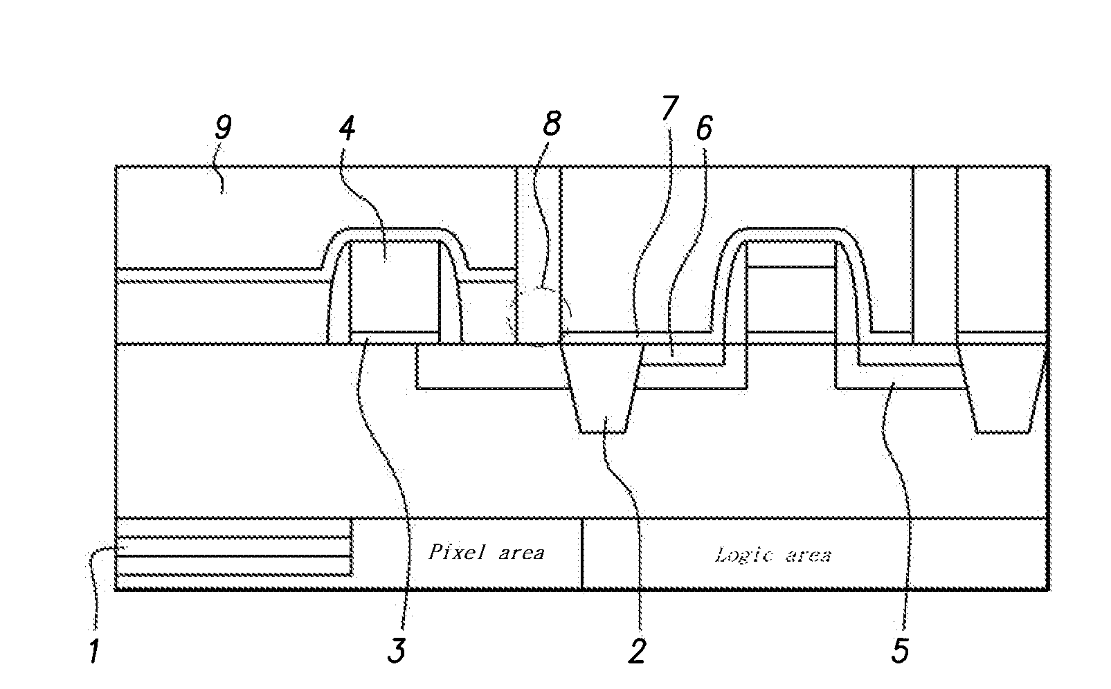
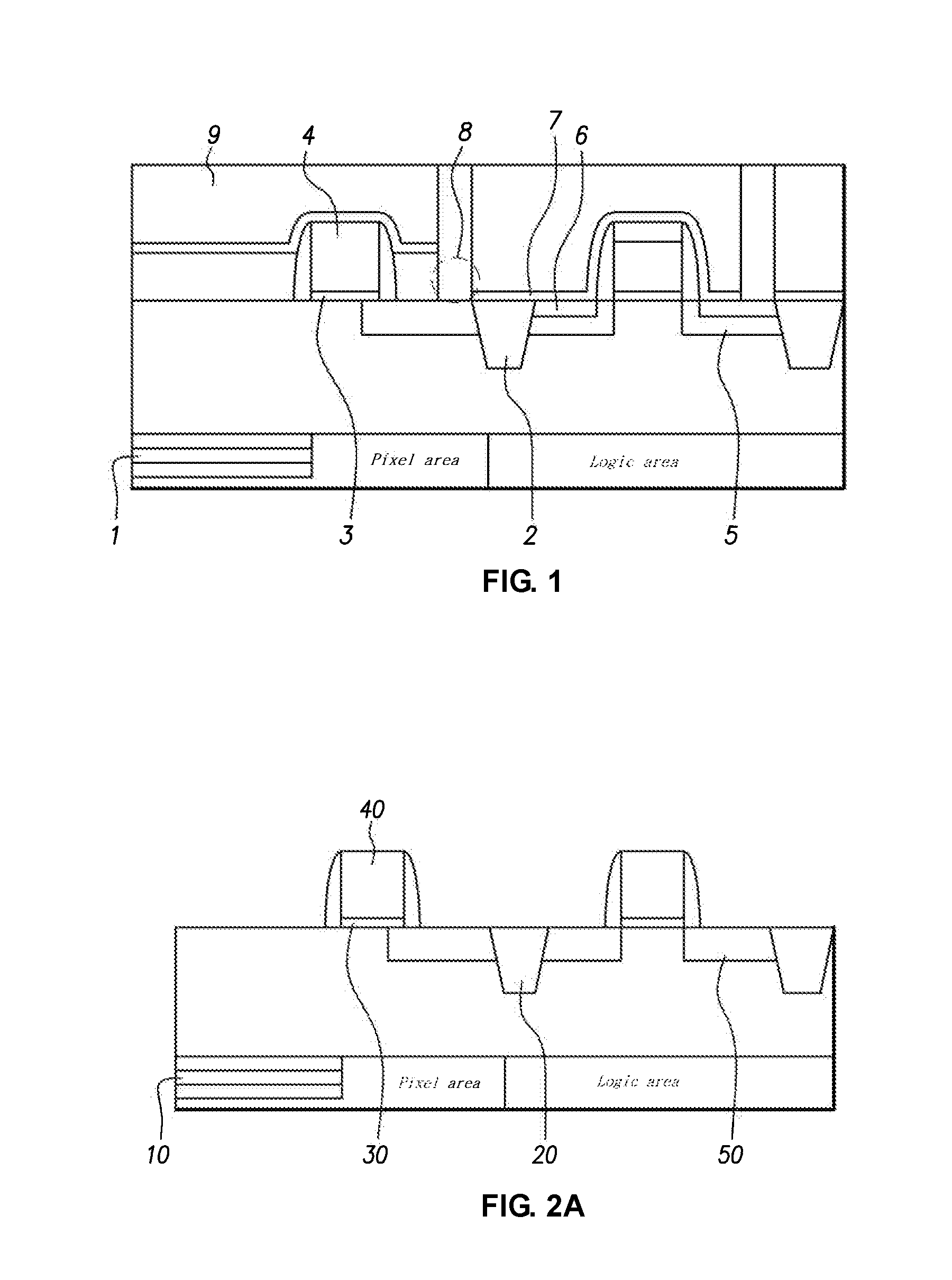
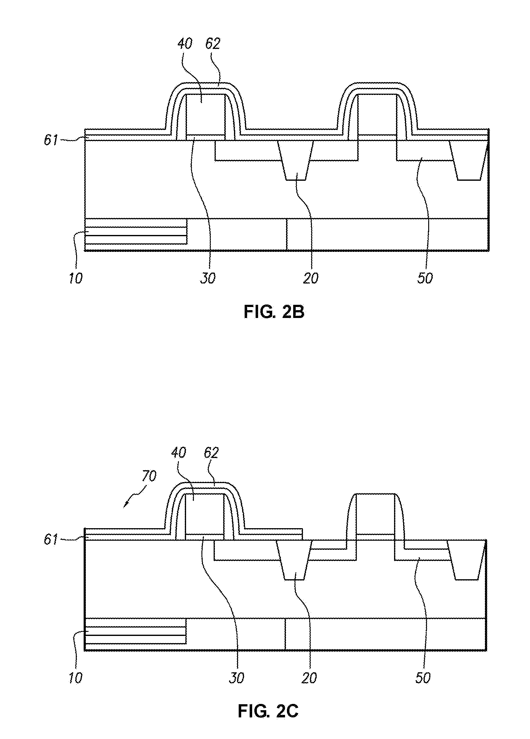
[0025]FIGS. 2A to 2E are cross-sectional diagrams illustrating a method of fabricating a CMOS image sensor according to one embodiment of the present invention, which show a borderless contact being formed in the non-salicide area by performing both salicidation and silicidation processes.

[0026]Referring to FIG. 2A, an epitaxial layer is formed on a semiconductor substrate by an epitaxy process.

[0027]Then, the epitaxial layer is divided into a pixel area including a plurality of photodiodes 10 and a logic area with a plurality of devices which are capable of signal processing. Next, an insulating layer is formed on the epitaxial layer. STI CMP is then carried out on the insulating layer to form an STI (shall...


PUM


Abstract

A method of fabricating a CMOS image sensor comprising forming an epitaxial layer on a semiconductor substrate, the epitaxial layer comprising a pixel and logic area, forming an STI layer in an insulating layer on the epitaxial layer, forming a plurality of wells and a gate pattern having a spacer on the insulating layer, forming a plurality of source and drain regions in the insulating layer using ion implantation, forming a salicide blocking layer on the insulating layer and gate pattern in the pixel area, forming a plurality of silicide layers in the logic area by performing a silicidation process, sequentially forming a PMD liner nitride layer and a PSG (phosphosilicate glass) layer on the salicide blocking layer in the pixel area and the insulating layer and gate pattern in the logic area, and forming a plurality of contacts connecting the PSG layer to the source and drain regions.

Description

CROSS-REFERENCES AND RELATED APPLICATIONS[0001]This application claims the benefit of the Korean Patent Application No. 10-2006-0137363, filed on Dec. 29, 2006, which is hereby incorporated by reference in its entirety.BACKGROUND OF THE INVENTION[0002]1. Field of the Invention[0003]The present invention relates to an image sensor. More particularly, the present invention relates to a CMOS image sensor and fabricating method the same.[0004]2. Discussion of the Related Art[0005]Generally, an image sensor is a device which is capable of converting an optical image into an electric signal. Within the image sensors industry, the sensors are typically categorized as either CMOS (complementary metal-oxide-silicon) image sensors or CCS (charge coupled device) image sensors.[0006]The CCD image sensors have superior noise and photo sensitivity characteristics when compared to the CMOS image sensors, but have difficulties achieving the density required for highly integrated systems and reducin...

Claims


Application Information

Patent Timeline
IPC IPC(8): H01L31/113H01L21/00
CPCH01L27/14609H01L27/14689H01L27/14687H01L27/146
Inventor LEE, SANG GI
Owner DONGBU HITEK CO LTD
Why Eureka
Try Eureka