Saddle Type Flash Memory Device and Fabrication Method Thereof

a flash memory device and saddle structure technology, applied in the direction of semiconductor devices, electrical devices, nanotechnology, etc., can solve the problems of reducing the interval between the cells, increasing the threshold voltage distribution, and reducing the gate length, so as to improve the ability of the control electrode to reach the channel, improve the write/erase characteristics, and speed up the erase speed

Active Publication Date: 2008-07-03
SEOUL NAT UNIV R&DB FOUND
View PDF6 Cites 43 Cited by
  • Summary
  • Abstract
  • Description
  • Claims
  • Application Information

AI Technical Summary

Benefits of technology

[0021]As described above, the present invention can realize a flash memory device in which a channel and gate structure has a saddle structure that solves problems with the existing devices.
[0022]Because the saddle-type device structure according to the present invention has a recessed channel structure and a triple-gate structure, it has all advantages with the existing double/triple-gate and advantages with the recessed channel structure. In addition to these advantages, the present invention provides the following additional advantages.
[0023]The existing bulk FinFET requires a fin body width corresponding to about ⅔ of the gate length, whereas the inventive structure has no problem even when making the body width equal to or thicker than the gate length, and can provide the advantages intended in the present invention. Also, the inventive structure can make erase speed through the body fast, improve write/erase characteristics by increasing the ability of the control electrode to the channel, reduce a change in threshold voltage resulting from back bias, redu

Problems solved by technology

Problems with the existing flash memory devices include: a short channel effect resulting from a decrease in gate length; the cross-talk between cells, resulting from a reduction in the interval between the cells; an increase

Method used


Image

  • Saddle Type Flash Memory Device and Fabrication Method Thereof
  • Saddle Type Flash Memory Device and Fabrication Method Thereof
  • Saddle Type Flash Memory Device and Fabrication Method Thereof

Examples


Embodiment Construction

[0050]Hereinafter, the construction and operation of embodiments of the present invention will be described in detail with reference to the accompanying drawings.

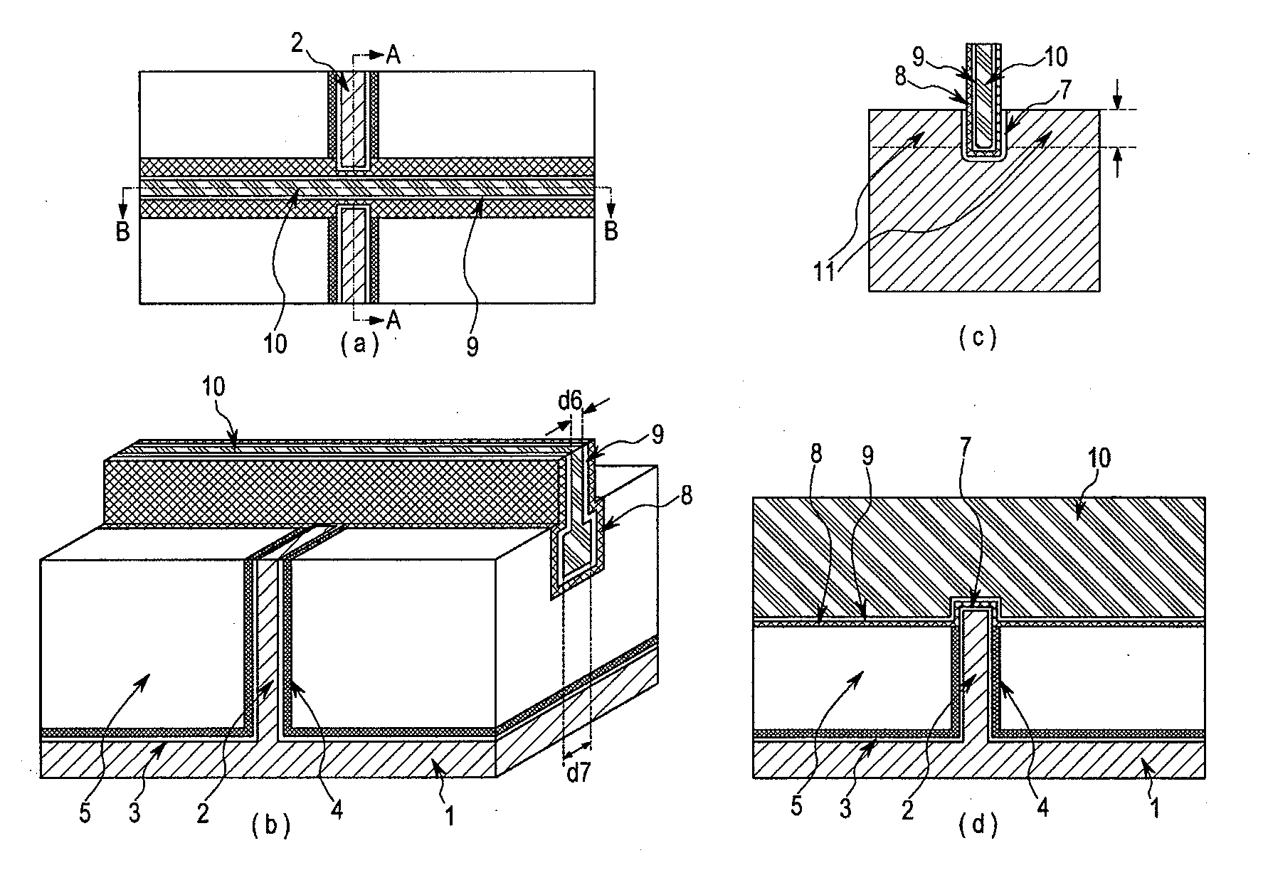
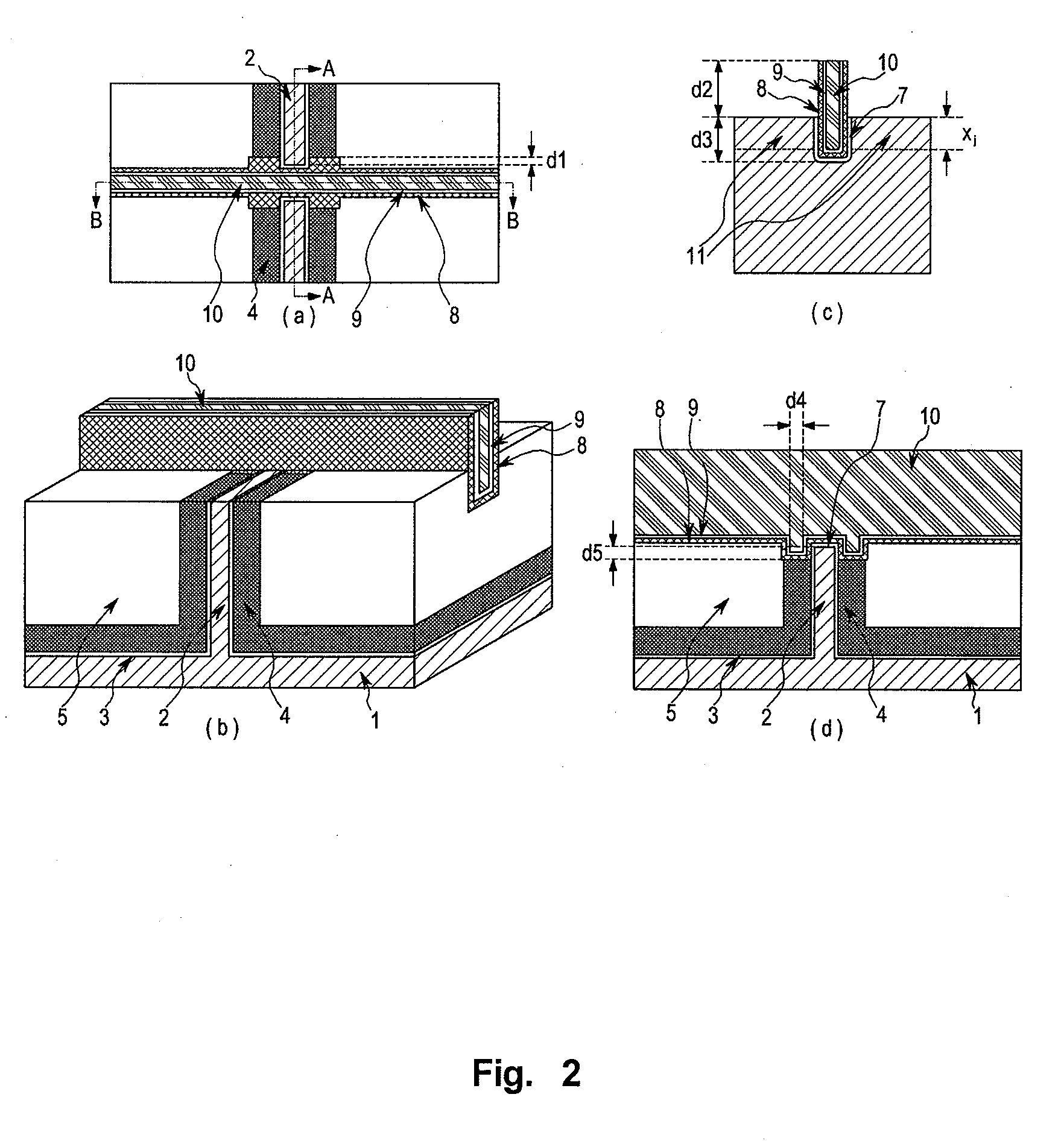
[0051]FIG. 2 shows a MOS device having a saddle structure according to the present invention. FIG. 2c is a cross-sectional view taken along an active region in line A-A of FIG. 2a, FIG. 2d is a cross-sectional view taken along a control electrode formed in the recessed channel region in line B-B of FIG. 2a. Also, the three-dimensional device structure shown in FIG. 2b shows important parts except for metal interconnections and source / drain contact regions.

[0052]FIG. 2 shows a structure just after forming a control electrode and source / drain regions, and subsequent steps are almost similar to CMOS processing technology. In FIG. 2b, region 1 is a silicon substrate, and region 2 is a wall-type silicon body in which an active channel region is formed. The thickness of the wall-type silicon body is suitably selected in a range o...


PUM


Abstract

The present invention relates to a nano-scale flash memory device having a saddle structure, and a fabrication method thereof. Particularly, the invention relates to a highly integrated, high-performance flash memory device having a saddle structure for improving the scaling-down characteristic and performance of the MOS-based flash memory device. According to the invention, a portion of an insulating film around a recessed channel is selectively removed to expose the surface and sides of the recessed channel. A tunneling insulating film is formed on the exposed surface and sides of the recessed channel. On the resulting structure, a floating electrode, an inter-electrode insulating film and a control electrode are formed, thus fabricating the device. Particularly when the floating electrode is made of an insulating nitride film or pluralities of nano-scale dots, an excellent memory device can be made without using an additional mask. According to the invention, the scaling-down characteristic of the device is excellent, and current drive capability can be greatly increased since a channel through which current can flow is formed on the surface and sides of the recessed channel. Also, the ability of the control electrode to control the channel can be enhanced, so that memory write/erase characteristics can be improved.

Description

TECHNICAL FIELD[0001]The present invention relates to a nano-scale flash memory device having a saddle structure, and a fabrication method thereof. More particularly, it relates to a highly integrated, high-performance flash memory device having a novel structure for improving the scaling-down characteristic and performance of the MOS-based flash memory device.BACKGROUND ART[0002]Recently, flash memory has been rapidly increasing in demand in household and portable electronic devices and is highly marketable, and thus is expected to exceed the existing DRAM market around the year 2007. Also, there is a continued need for memory devices having high integration density and fast write / erase time.[0003]The existing flash memory devices are devices having a channel formed on a silicon surface. These devices seem to reach a limit between 45-60 nm technologies depending on memory types (NOR type or NAND type), and they require a device structure which has high performance and integration d...

Claims


Application Information

Patent Timeline
IPC IPC(8): H01L29/788H01L21/336
CPCB82Y10/00H01L21/28273H01L21/28282H01L29/42332H01L29/42336H01L29/42352H01L29/792H01L29/66825H01L29/66833H01L29/7781H01L29/785H01L29/7854H01L29/66795H01L29/40114H01L29/40117H01L21/18H01L21/28H10B99/00
Inventor LEE, JONG-HO
Owner SEOUL NAT UNIV R&DB FOUND
Why Eureka
Try Eureka