Circuit board structure having electronic components integrated therein

a technology of electronic components and circuit boards, applied in the direction of electrical apparatus contruction details, printed circuit non-printed electric components association, semiconductor/solid-state device details, etc., can solve the problems of inability to proceed, unsuitable conventional technology for large-scale thin-substrat panel fabrication, and cracking of core board panels, so as to reduce the possibility of panel cracking, enhance the structural rigidity of the circuit board, and prevent warpage

Active Publication Date: 2008-07-10
UNIMICRON TECH CORP
View PDF10 Cites 12 Cited by
  • Summary
  • Abstract
  • Description
  • Claims
  • Application Information

AI Technical Summary

Benefits of technology

[0008]In light of the foregoing drawbacks of the prior all, a primary objective of the present invention is to provide a circuit board having electronic components integrated therein for enhancing the structural rig

Problems solved by technology

However since ceramic core board, panel is brittle in property, it may crack once the stress is larger than that the panel can sustain.
In typical fabrication of the core board made of ceramic, as the ceramic panel has a poor flexibility when the sum of stress of the unsymmetrical built-up structures is larger than the limit the core board panel can sustain, the core board panel may crack, and unable to proceed to the following processes.
Thus, the conventional technology is s

Method used


Image

  • Circuit board structure having electronic components integrated therein
  • Circuit board structure having electronic components integrated therein
  • Circuit board structure having electronic components integrated therein

Examples


first embodiment

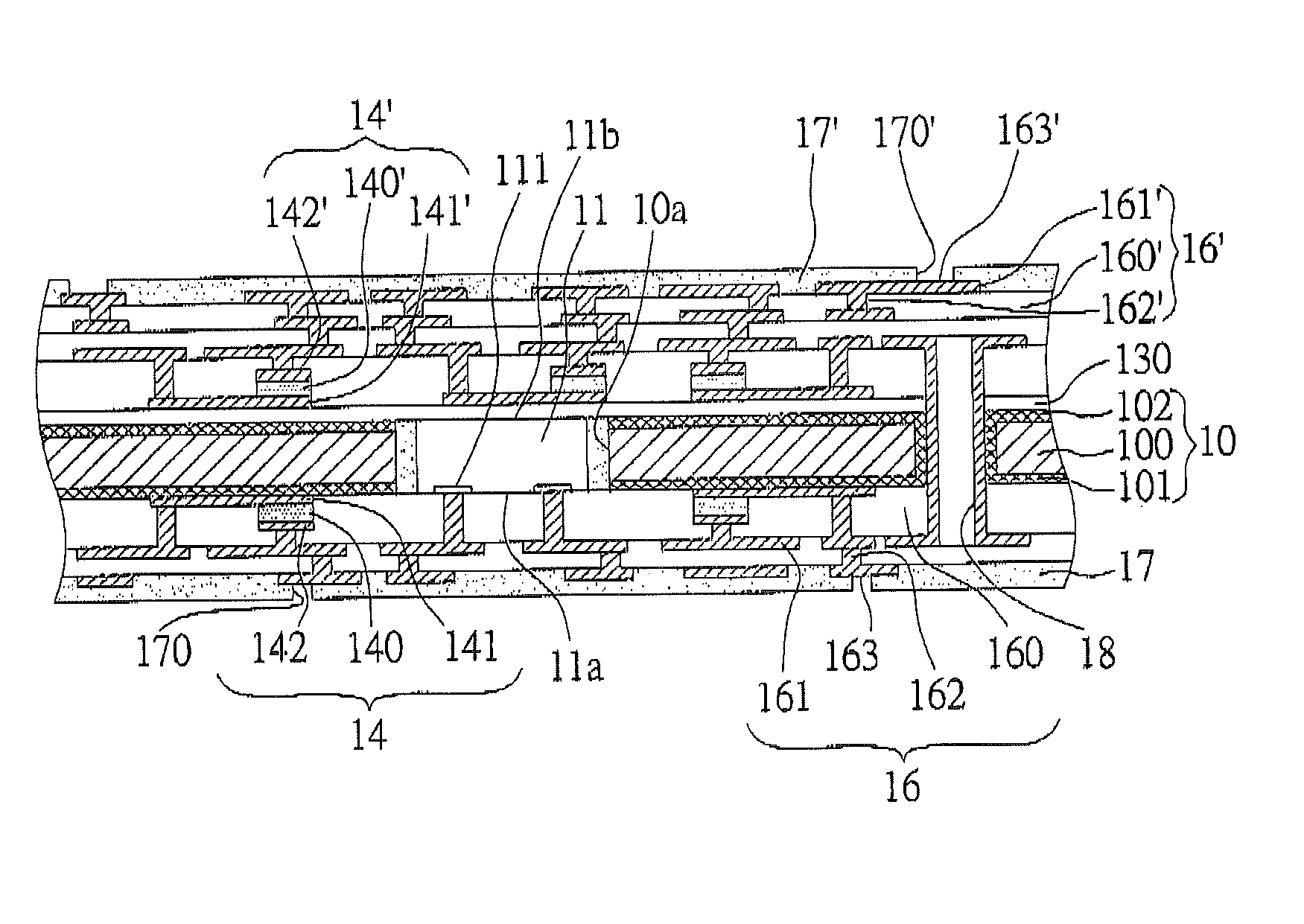
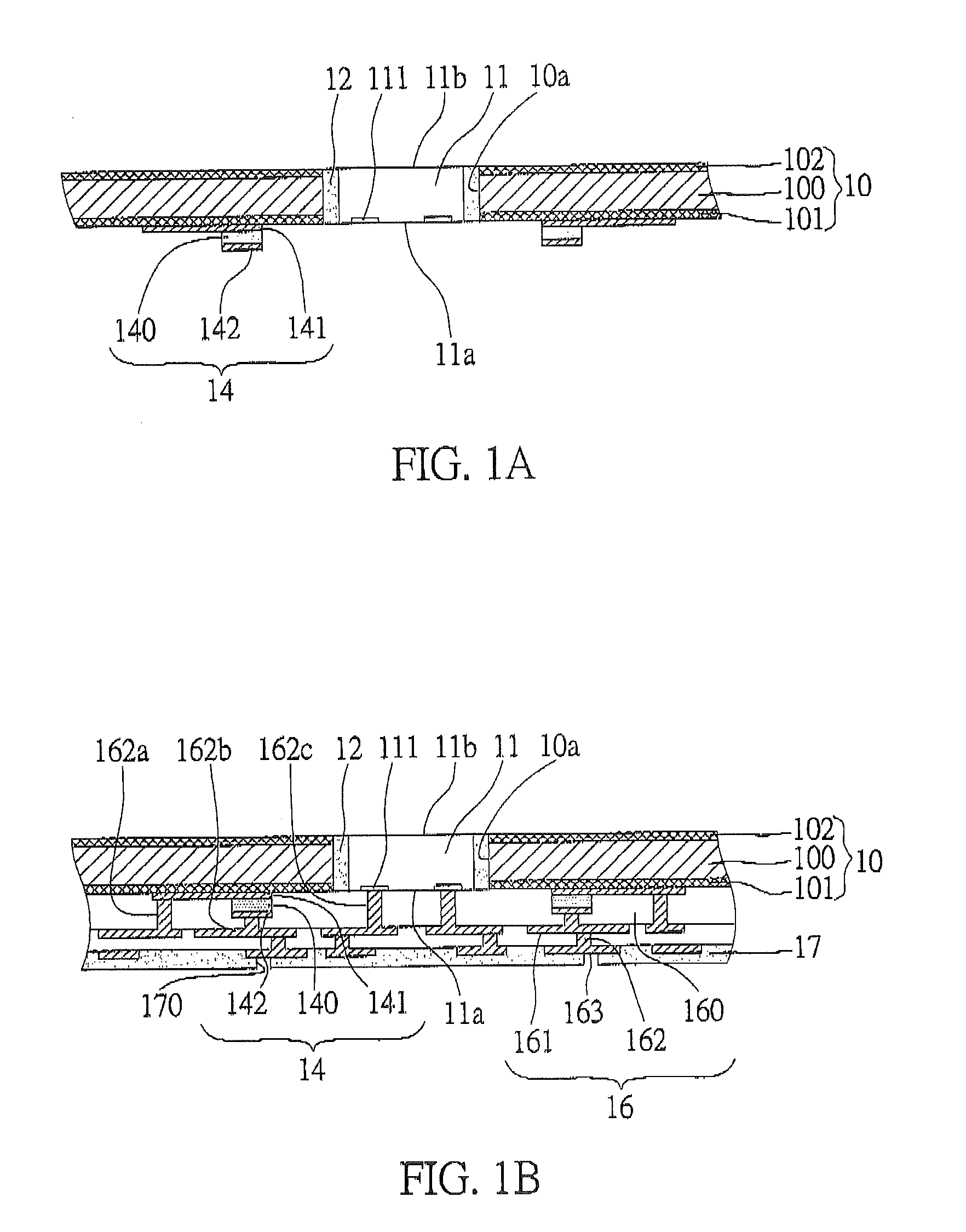
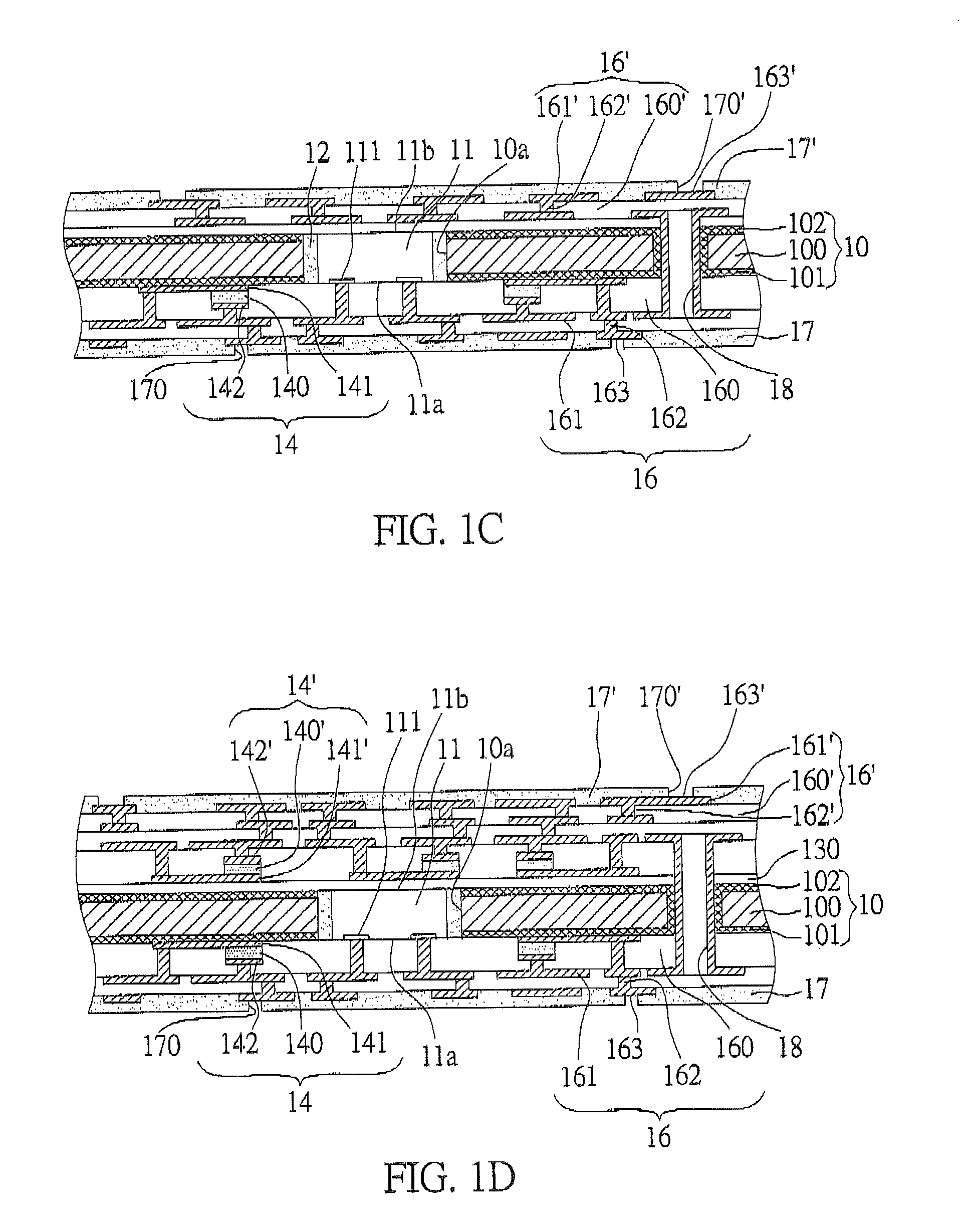
[0031]Referring to FIGS. 1A-1D, cross-sectional schematic views of a circuit board having electronic components integrated therein of the present invention are shown.

[0032]As shown in FIG. 1A, the circuit board having electronic components integrated therein comprises: a carrier board 10, at least one semiconductor chip 11 and a capacitor 14. The carrier board 10 is formed by respectively forming a first metallic oxide layer 101 and a second metallic oxide layer 102 on two sides of a metal layer 102. The metal layer 100 is made of aluminum which is oxidized to form the first metallic oxide layer 101 and second metallic oxide layer 102 on each side respectively for enhancing the rigidity of the carrier board 10. Moreover, the carrier board 10 has at least one through cavity 10a penetrating the carrier board 10. The semiconductor chip 11 is hold in the through cavity 10a of the carrier board 10. The semiconductor chip 11 has an active surface 11a with a plurality of electrode pads 111...

second embodiment

[0038]Referring to FIGS. 3A-3D, the difference between the second embodiment and the first embodiment is that the second embodiment further comprises a dielectric layer 131 disposed between the active surface 11a of the semiconductor chip 11 (together with the surface of the carrier board 10 at the same side) and the capacitors 14 for providing a better bonding between the capacitor 14 and the carrier board 10. Further referring to FIG. 4A-4D, in this embodiment, the dielectric layer 131 can replace the adhesive material to fill the gap between the through cavity 10a of the carrier board 10 and the semiconductor chip 11, so as to fix the semiconductor chip 11 in the through cavity 10a. Other main components in this embodiment can be referred to that of the first embodiment, therefore not given herein.

third embodiment

[0039]FIG. 5 shows a cross-sectional view of the circuit board having electronic components integrated therein of the third embodiment of the invention. The difference of this embodiment from the other embodiments is that in this embodiment the active surface 11a of the semiconductor chip 11 is at the same side with the second metallic oxide layer 102 of the carrier board 10. The circuit board structure comprises: a carrier board. 10 which is formed by respectively forming a first metallic oxide layer 101 and a second metallic oxide layer 102 on two sides of a metal layer 102, and, a through cavity 10a penetrating the carrier board; at least one semiconductor chip 11 having an active surface 11a with a plurality of electrode pads 111 thereon and an inactive surface 11b, hold in the through cavity 10a, wherein the active surface 11a of the semiconductor chip 11 is at the same side with the second metallic oxide layer 102; an adhesive material 12 filling the gap between the through ca...


PUM


Abstract

The present invention provides a circuit board having electronic components integrated therein, including a carrier board having an metallic oxide layer formed on each two surfaces of a metal layer, and having at least one through cavity; at least a semiconductor chip hold in the opening; at least a capacitor disposed on one surface of the carrier board, wherein the surface with the capacitor disposed thereon is at the same side with the active surface of the semiconductor chip. The capacitor is constituted of a first electrode plate disposed on partial surface of one side of the carrier board, a high dielectric material layer disposed on the surface of the first electrode plate, and a second electrode plate, paralleling and corresponding to the first electrode plate, disposed on the surface of the high dielectric material. The metal layer and the oxidation layer of the carrier board can enhance rigidity as well as tenacity and also integrate semiconductor chips and capacitors in the circuit board structure.

Description

BACKGROUND OF THE INVENTION[0001]1. Field of the invention[0002]The present invention relates to a circuit board having electronic components integrated therein, and more particularly to a circuit board having semiconductor chips and capacitors integrated therein.[0003]2. Description of the Prior Art[0004]A semiconductor package in which electronic components are embedded in the substrate is developed in the semiconductor industry along with the trend towards low-profile and light-weighted electronic devices. For examples, typically a circuit board structure with embedded electronic components are formed by embedding active components such as semiconductor chips, or inactive components such as resistors, capacitors, and inductors in the substrate followed by forming circuits on the substrate. On the other hand, ceramic materials are often chosen in the fabrication of the substrate due to its high Young's modulus therefore better rigidity.[0005]Since the ceramic substrate has a bette...

Claims


Application Information

Patent Timeline
IPC IPC(8): H05K7/00
CPCH01L23/50H01L2924/01033H01L24/19H01L2224/04105H01L2224/20H01L2924/01013H01L2924/18162H01L2924/19041H01L2924/19042H01L2924/19043H05K1/053H05K1/162H05K1/185H05K3/4608H05K2201/09509H05K2201/09763H05K2201/10674H01L23/5389H01L2224/73267H01L2924/15787H01L2924/00
Inventor HSU, SHIH-PINGCHIA, KAN-JUNG
Owner UNIMICRON TECH CORP
Why Eureka
Try Eureka