Layout structure of semiconductor integrated circuit

a technology of integrated circuits and layout structures, applied in semiconductor devices, semiconductor/solid-state device details, electrical devices, etc., can solve the problems of reducing the flexibility of adjusting the source resistance, and the reduction of the operating speed of a semiconductor integrated circuit, so as to improve the flexibility of the arrangement of ca vias in the source diffusion region, the effect of improving the flexibility of design of a transistor having a higher operating speed

Inactive Publication Date: 2008-07-17
PANASONIC CORP
View PDF6 Cites 53 Cited by
  • Summary
  • Abstract
  • Description
  • Claims
  • Application Information

AI Technical Summary

Benefits of technology

[0066]According to the present invention, in order to solve the first problem, an inter-drain wiring which is formed in a wiring layer different from that of a power source wiring is provided between drain terminals. Therefore, a CA via can be provided even in a portion of the source diffusion region on which the inter-drain wiring is provided. Therefore, as compared to the first conventional example, the flexibility of arrangement of a CA via in the source diffusion region is improved, and therefore, the flexibility of adjustment of source resistance by changing the number of CA vias is also improved, so that the flexibility of design of a transistor having a higher operating speed is improved.
[0067]Also, according to the present invention, in order to solve the second problem, a standard cell is provided which includes two kinds of diffusion regions, i.e., a broad diffusion region in which a plurality of CA vias can be arranged in a horizontal direction, and a diffusion region narrower than the broad diffusion region, without leading to variations in gate length. Therefore, by using the broad diffusion region as a source diffusion region and the narrow diffusion region as a drain diffusion region, a plurality of CA vias can be provided in the source diffusion region without an in

Problems solved by technology

On the other hand, an advance in the miniaturization has led to two significant problems which directly cause a reduction in operating speed.
A first problem is that the operating speed of a semiconductor integrated circuit decreases due to variations in gate length.
A second problem is that the operating speed of a semiconductor integrated circuit decreases due to an increase in resistance of a CA via for the source of a transistor.
The first problem arises during the exposure step.
In this case, if the circuit pattern is excessively fine, the circuit pattern acts on light waves as if it were a diffraction grating, so that scattered light occurs.
As a result, a significant error occurs in the shape of the transferred circuit pattern.
The shape error increases with a decrease in width or pitch of a pattern drawn on a mask.
The gate length of a transistor is strongly affected by the shape error.
If this mask is used to perform exposure, a gate wiring having a certain amount of shape error is formed on a silicon substrate due to the influence of scattered light.
The gate length of a transistor having a narrow gate wiring pitch has a large shape error on the silicon substrate since it is largely affected by scattered light.
On the other hand, the gate length of a transistor having a broad gate wiring pitch has a small shape error on the silicon substrate since it is less affected by scattered light.
As described above, if a semiconductor integrated circuit comprising transistors having varying gate wiring pitches is formed on a silicon substrate, then when the transistors are transferred from a mask to a silicon wafer, the gate lengths of the transistors are not uniform, i.e., the gate lengths have a certain amount of variation.
Since the operating speed of a semiconductor integrated circuit varies from a value estimated during a design stage, it is difficult to obtain a semiconductor integrated circuit having a desired operating speed.
As described above, if an attempt is made to produce a semiconductor integrated circuit having transistors with varying gate wiring pitches using an advanced miniaturization process, the operating speed of the semiconductor integrated circuit is easily deteriorated.
A metal wiring having a larger resistance value leads to a decrease in propagation speed of a signal propagating through the metal wiring, or a break in the metal wiring due to heat.
However, when copper contacts a silicon substrate, copper is diffused into the silico

Method used


Image

  • Layout structure of semiconductor integrated circuit
  • Layout structure of semiconductor integrated circuit
  • Layout structure of semiconductor integrated circuit

Examples


first example

Variation of First Example

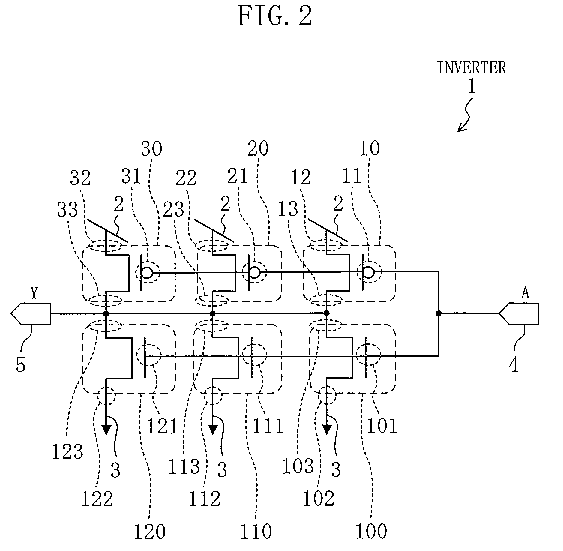
[0095]FIG. 2 shows a variation of the first example in which the present invention is applied to an inverter which is a semiconductor integrated circuit.

[0096]In FIG. 2, the inverter 1 includes P-channel transistors 10, 20 and 30, and N-channel transistors 100, 110 and 120. The gate terminals 11, 21 and 31 of the P-channel transistors 10, 20 and 30 are all connected to an input terminal 4. The source terminals 12, 22 and 32 of the P-channel transistors 10, 20 and 30 are all connected to a VDD power source 2. The VDD power source 2 has a predetermined potential VDD.

[0097]The drain terminals 13, 23 and 33 of the P-channel transistors 10, 20 and 30 are all connected to an output terminal 5. The gate terminals 101, 111 and 121 of the N-channel transistors 100, 110 and 120 are all connected to the input terminal 4. The source terminal 102, 112 and 122 of the N-channel transistor 100, 110 and 120 are all connected to a VSS power source 3. The VSS power source 3 h...

second example

[0112]FIG. 4 shows a standard cell according to a second example of the present invention. FIG. 5 shows a layout structure of a semiconductor integrated circuit using the standard cell of FIG. 4. Hereinafter, FIGS. 4 and 5 will be described in detail.

[0113]Firstly, FIG. 4 will be described. In FIG. 4, the standard cell 400 comprises a P-type diffusion region 401 and an N-type diffusion region 402. Gate wirings 404 to 409 with a wiring width L are arranged in a direction perpendicular to the upper and lower sides of the standard cell 400. The gate wirings 404 to 409 of P-channel transistors P404 to P409 and N-channel transistors N404 to N409 have a first wiring pitch S0 and a second wiring pitch S1, which are alternately repeated. Specifically, a wiring pitch between the gate wiring 405 and the gate wiring 406 is the first wiring pitch S0, and a wiring pitch between the gate wiring 406 and the gate wiring 407 is the second wiring pitch S1. A wiring pitch between the gate wirings of t...

third example

[0151]FIG. 6 shows a standard cell according to a third example of the present invention. FIG. 7 shows a semiconductor integrated circuit employing the standard cell of FIG. 6.

[0152]Firstly, FIG. 6 will be described. In FIG. 6, the standard cell 600 is the standard cell of FIG. 12 which comprises an OR logic. The left and ride sides of the standard cell 600 has a length 610 which is two times higher than the width of a standard cell row. The standard cell 600 is referred to as a double-height cell. The double-height cell 600 comprises two standard cells 601 and 602 which are vertically linked together with the lower side of the standard cell 601 and the upper side of the standard cell 602 contact each other.

[0153]In the standard cell 601, transistors are arranged in a manner such that a gate wiring pitch thereof is a single constant first wiring pitch S. The standard cell 601 corresponds to the NOR circuit 2010 of FIG. 12.

[0154]On the other hand, in the standard cell 602, transistor...


PUM


Abstract

In a layout structure of a semiconductor integrated circuit, when transistors are arranged in a constant gate wiring pitch, a common source diffusion region is provided between two adjacent transistors, a CA via is provided on the common source diffusion region, and a source wiring connected to the CA via is provided on the common source diffusion region. An inter-drain wiring connecting the drain regions of the two transistors is formed in a wiring layer higher than the source wiring. Therefore, the wiring path of the source wiring is not limited by the wiring path of the inter-drain wiring, and can be provided, covering the common source diffusion region to a further extent. As a result, the number of high-resistance CA vias or the flexibility of arrangement is increased, leading to a reduction in source resistance, resulting in an increase in operating speed of the semiconductor integrated circuit.

Description

CROSS REFERENCE TO RELATED APPLICATIONS[0001]This Non-provisional application claims priority under 35 U.S.C. §119(a) on Patent Application No. 2007-003184 filed in Japan on Jan. 11, 2007, the entire contents of which are hereby incorporated by reference.BACKGROUND OF THE INVENTION[0002]1. Field of the Invention[0003]The present invention relates to a layout structure of a semiconductor integrated circuit employing standard cells which are each a base unit in the layout of the semiconductor integrated circuit. More particularly, the present invention relates to a layout structure of a semiconductor integrated circuit employing standard cells which have a constant gate wiring pitch of transistors.[0004]2. Description of the Related Art[0005]Conventionally, in order to achieve a low-cost and high-performance semiconductor integrated circuit, attempts have been made to reduce the area of each individual semiconductor integrated circuit to the extent possible without reducing the operat...

Claims


Application Information

Patent Timeline
IPC IPC(8): H01L27/10
CPCH01L27/0207
Inventor SHIMBO, HIROYUKINISHIMURA, HIDETOSHI
Owner PANASONIC CORP
Why Eureka
Try Eureka