Method for fabricating bottom-gate low-temperature polysilicon thin film transistor

a thin film transistor and low-temperature technology, applied in the direction of semiconductor devices, basic electric elements, electrical equipment, etc., can solve the problems of reducing carrier mobility and electric performance, affecting the performance of existing polysilicon layers, and blending too many tiny crystal grains with big crystal grains, so as to promote carrier mobility

Inactive Publication Date: 2008-07-17
CHENG HUANG CHUNG +2
View PDF3 Cites 13 Cited by
  • Summary
  • Abstract
  • Description
  • Claims
  • Application Information

AI Technical Summary

Benefits of technology

[0007]The primary objective of the present invention is to provide a method for fabricating a bottom-gate low-temperature polysilicon thin film transistor, whereby polysilicon grains grow laterally in the channel of the active region, and the carriers thus pass through fewer grain boundaries when they cross the active region, and the carrier mobility is thus promoted.
[0008]Another objective of the present invention is to provide a method for fabricating a bottom-gate low-temperature polysilicon thin film transistor, whereby polysilicon grains grow laterally in the channel of the active region, and the interface between the active region and the gate insulating layer becomes smoother.
[0009]Yet another objective of the present invention is to provide a method for fabricating a bottom-gate low-temperature polysilicon thin film transistor, whereby the transistor has a superior element motive force and a steeper subthreshold swing.
[0010]Further another objective of the present invention is to provide a method for fabricating a bottom-gate low-temperature polysilicon thin film transistor, which can fabricate a high-performance transistor simply with a thinner gate oxide layer and can promote the competitiveness of the display products when the transistors fabricated according to the present invention are used as the switch elements of the pixel circuit.

Problems solved by technology

Besides, too many tiny crystal grains blend with big crystal grains.
Thus, the carrier mobility and the electric performance are reduced.
Further, in such a conventional transistor structure, the existing polysilicon layer is likely to be damaged by the photolithographic process for fabricating the top oxide layer 18 and the top gate 20.

Method used


Image

  • Method for fabricating bottom-gate low-temperature polysilicon thin film transistor
  • Method for fabricating bottom-gate low-temperature polysilicon thin film transistor
  • Method for fabricating bottom-gate low-temperature polysilicon thin film transistor

Examples


Embodiment Construction

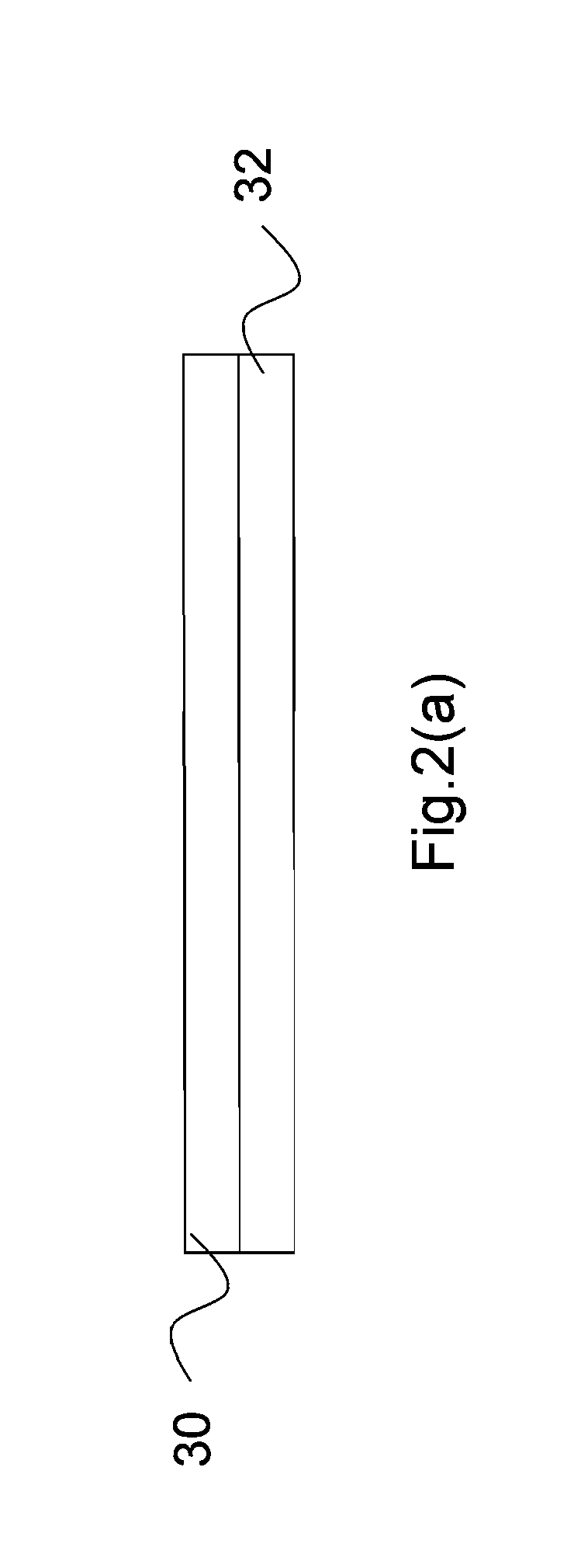
[0021]Refer to from FIG. 2(a) to FIG. 2(e) diagrams schematically showing the steps of fabricating a low-temperature polysilicon layer on a substrate with a bottom gate according to the present invention.

[0022]As shown in FIG. 2(a), a silicon substrate 32 with an oxide layer 30 is provided; alternatively, the substrate may be made of a glass or plastic. Next, as shown in FIG. 2(b), a gate layer 34 is formed on the oxide layer 30; the gate layer 34 may be a metal layer; alternatively, the gate layer 34 may be obtained via the following steps: decomposing monosilane (SiH4) and hydrogen phosphide (PH3) at 550° C. to form a phosphorus-doped polysilicon layer with a low-temperature CVP (Chemical Vapor Deposition) method, and fabricating the polysilicon layer into the gate layer 34 having the designed pattern with a photolithographic process, wherein the photolithographic process can be implemented with a transformer coupled plasma, and the gate layer 34 has a thickness of between 30 and ...


PUM

PropertyMeasurementUnit
thicknessaaaaaaaaaa
thicknessaaaaaaaaaa
thicknessaaaaaaaaaa

Abstract

The present invention discloses a method for fabricating a bottom-gate low-temperature polysilicon thin film transistor, wherein the bottom gate structure is used to form an amorphous silicon layer with varied thicknesses; the amorphous silicon layer in the step region on the border of the bottom gate structure is partially melted by an appropriate amount of laser energy; the partially-melted amorphous silicon layer in the step region functions as crystal seeds and makes crystal grains grow toward the channel region where the amorphous silicon layer is fully melted, and the crystal grains are thus controlled to grow along the lateral direction to form a lateral-grain growth low-temperature polysilicon thin film. The lateral grain growth can reduce the number of the grain boundaries carriers have to pass through. Thus, the present invention can promote the carrier mobility in the active region and the electric performance. Further, the present invention can achieve a superior element motive force and a steeper subthreshold swing.

Description

BACKGROUND OF THE INVENTION[0001]1. Field of the Invention[0002]The present invention relates to a method for a low-temperature polysilicon thin film transistor, particularly to a method for fabricating a bottom-gate low-temperature polysilicon thin film transistor.[0003]2. Description of the Related Art[0004]Owing to the superior carrier mobility, capability of being formed on a glass substrate, and capability of integrating with a display panel to reduce cost and achieve a high resolution, the low-temperature polysilicon TFT (Thin Film Transistor) has gradually replaced the traditional amorphous silicon TFT and become a critical element in display devices recently.[0005]Refer to FIG. 1 a diagram schematically showing a conventional top-gate low-temperature polysilicon TFT. The conventional top-gate low-temperature polysilicon TFT comprises a substrate 10, a first oxide layer 12 above the substrate 10, a polysilicon channel 14 above the first oxide layer 12, source / drain regions 16...

Claims


Application Information

Patent Timeline
Patent Type & Authority Applications(United States)
IPC IPC(8): H01L21/336
CPCH01L21/02532H01L21/02683H01L21/02686H01L29/78696H01L29/04H01L29/66765H01L27/1281
Inventor CHENG, HUANG-CHUNGTSAI, CHUN-CHIENCHEN, HSU-HSIN
Owner CHENG HUANG CHUNG
Why Eureka
Try Eureka