Method for forming contact hole
a contact hole and etching technology, applied in the field of semiconductor/solid-state device manufacturing, electrical equipment, basic electric elements, etc., can solve the problems of unstable electrical performance of the device, difficult to remove the polymer residue and the etching byproduct from such a narrow contact hole, and reduce the reliability of the devi
- Summary
- Abstract
- Description
- Claims
- Application Information
AI Technical Summary
Benefits of technology
Problems solved by technology
Method used
Image


Examples
Embodiment Construction
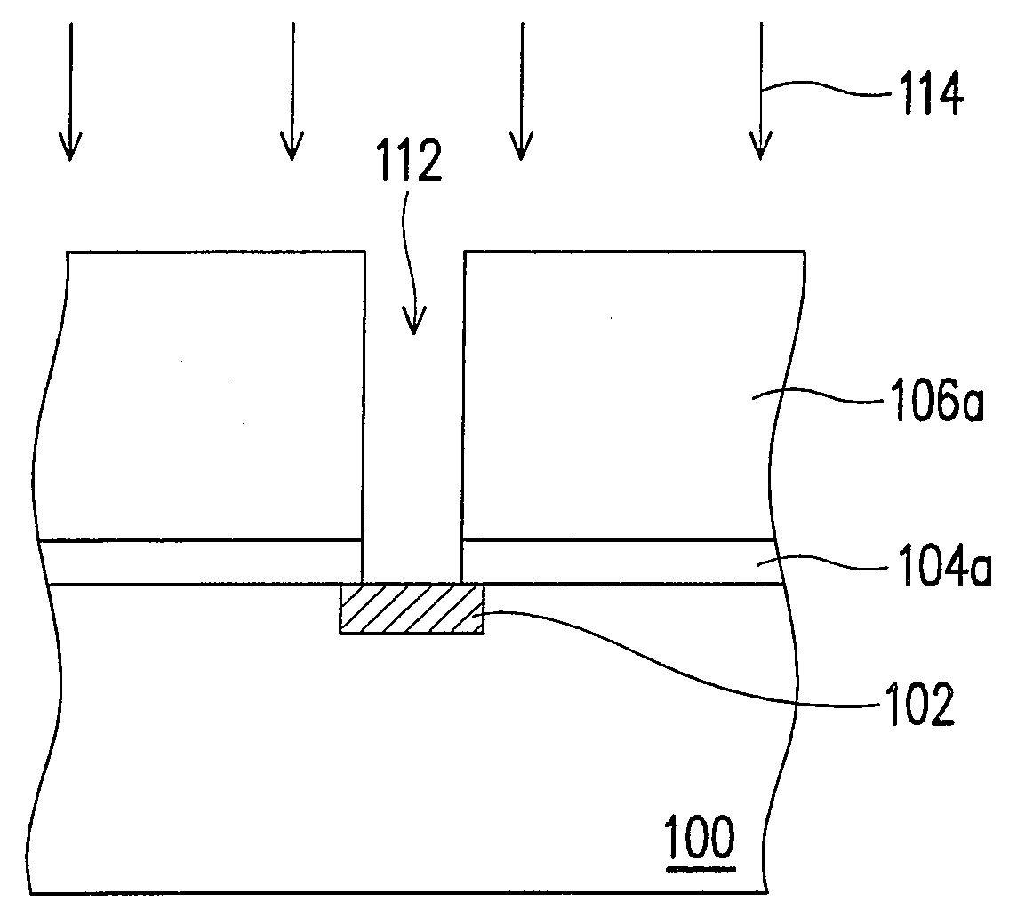
[0021]FIGS. 1A through 1C are cross-sectional views slowing a method for forming a contact hole according to one embodiment of the present invention. FIG. 2 is a flow chart showing a method for forming a contact hole according to one embodiment of the present invention. As shown in FIG. 1A and FIG. 2, in the step S201, a substrate 100 is provided. The substrate 100 has at least one dielectric layer 106 formed thereon. Furthermore, a contact etching stop layer 104 is disposed between the dielectric layer 106 and the substrate 100. Also, below the contact etching stop layer 104, there is a conductive layer 102. The conductive layer 102 can be, for example, made of metal silicide such as nickel silicide or cobalt silicide. Then, a patterned mask layer 108 is formed over the substrate 100 (step S203). The patterned mask layer 108 can be, for example, made of photoresist.
[0022]As shown in FIG. 1B together with FIG. 2, the dielectric layer 106 is patterned to form a contact hole 112 (show...
PUM
 Abstract
Description
Claims
Application Information
 - R&D
- Intellectual Property
- Life Sciences
- Materials
- Tech Scout
- Unparalleled Data Quality
- Higher Quality Content
- 60% Fewer Hallucinations
Browse by: Latest US Patents, China's latest patents, Technical Efficacy Thesaurus, Application Domain, Technology Topic, Popular Technical Reports.
© 2025 PatSnap. All rights reserved.Legal|Privacy policy|Modern Slavery Act Transparency Statement|Sitemap|About US| Contact US: help@patsnap.com