Plasma-enhanced ald of tantalum nitride films

a technology of tantalum nitride and plasma, which is applied in the direction of coating, metallic material coating process, chemical vapor deposition coating, etc., can solve the problems of affecting the electrical properties of the ic, difficult to obtain complete film coverage on the deep bottom and via, and prone to diffusion or electromigration

Active Publication Date: 2008-07-31
ASM IP HLDG BV
View PDF50 Cites 337 Cited by
  • Summary
  • Abstract
  • Description
  • Claims
  • Application Information

AI Technical Summary

Problems solved by technology

Design rules are setting the feature sizes to ≦0.2 μm, making complete film coverage on deep bottoms and vias difficult to obtain.
Cu is particularly prone to diffusion or electromigration into surrounding materials.
Diffusion may adversely affect the electrical properties of the IC, causing active components to malfunction.
While it may be desirable to use a plasma-enhanced process for depositing metal nitrides, if one of the reactants in the three-step ALD method disclosed in the '727 patent is substituted with a plasma-excited species, conductive metal nitride films (e.g., MN, where M is a metal and N is nitrogen), are formed throughout the reaction space, leading to electrical shorts that may impede, even prevent, plasma generation.
This can lead to significant downtime and an increase in processing costs.

Method used


Image

  • Plasma-enhanced ald of tantalum nitride films
  • Plasma-enhanced ald of tantalum nitride films

Examples


example

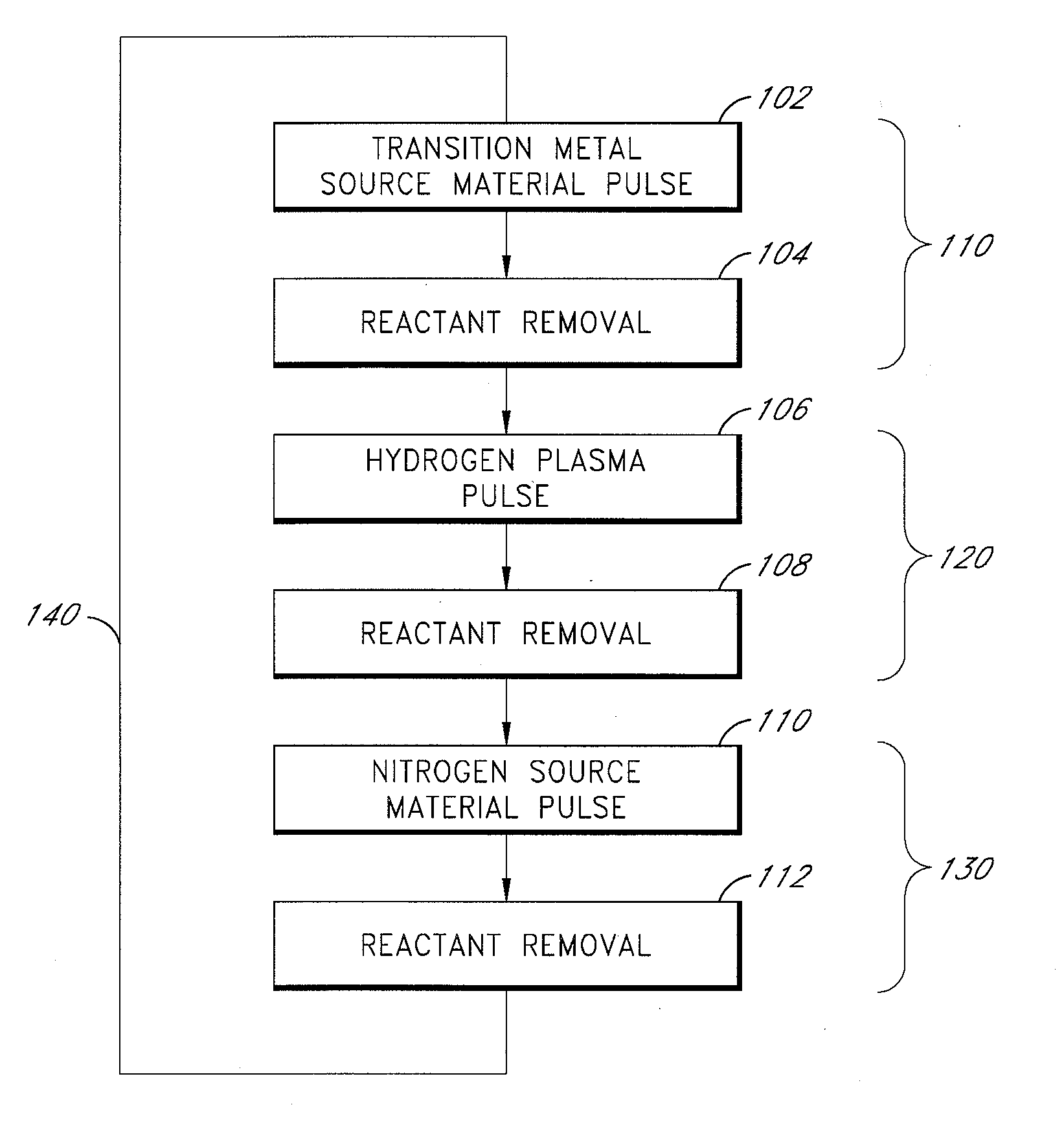
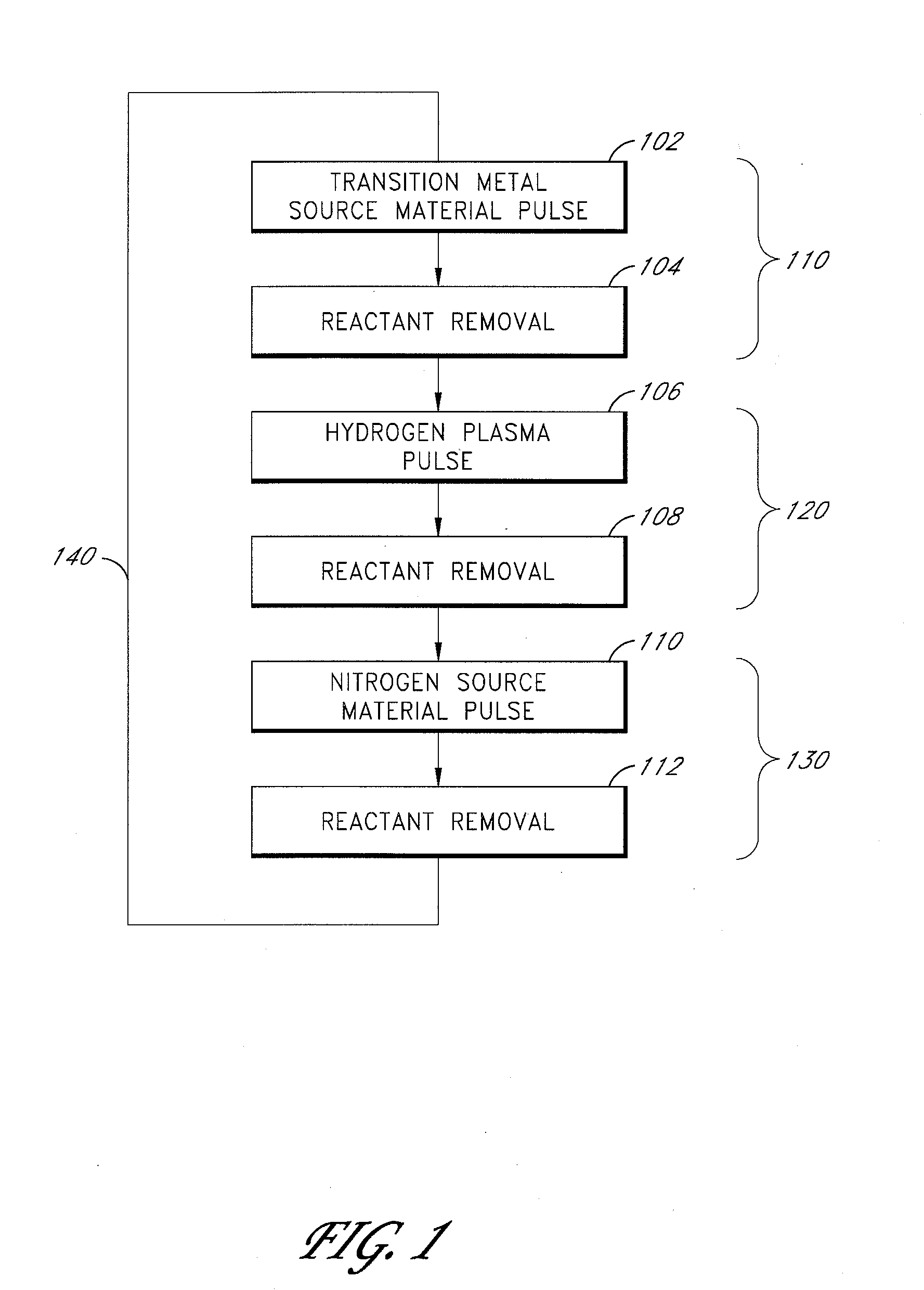
[0073]A conductive tantalum nitride film was deposited on a 300 mm silicon wafer in a PEALD reactor from ASM Genitech, Inc. Deposition was conducted at a substrate temperature of about 300-350° C. and a TaF5 source gas temperature of about 93° C. Hydrogen (H2) plasma and ammonia (NH3) were used as the reducing agent and nitrogen source material, respectively. H2 plasma was generated by pulsing H2 into the reactor and supplying power to a plasma generator (1 KW, 13.56 MHz) while holding the plasma power at about 400 W. The sequence of gas pulses and pulsing times (milliseconds, “ms”) are as follows:

[0074](1) TaF5 pulse (900 ms);

[0075](2) Ar purge (3000 ms);

[0076](3) H2 Plasma pulse (2000-4000 ms);

[0077](4) Ar purge (2000 ms);

[0078](5) NH3 pulse (1000-4000 ms); and

[0079](6) Ar purge (6000 ms);

[0080]Steps (1)-(6) were repeated until a conductive tantalum nitride film of thickness between about 40 nm and 70 nm was formed on the substrate. During the pulsing sequence, a throttle valve wa...


PUM

PropertyMeasurementUnit
feature sizesaaaaaaaaaa
thicknessaaaaaaaaaa
thicknessaaaaaaaaaa

Abstract

Methods of controllably producing conductive tantalum nitride films are provided. The methods comprise contacting a substrate in a reaction space with alternating and sequential pulses of a tantalum source material, plasma-excited species of hydrogen and nitrogen source material. The plasma-excited species of hydrogen reduce the oxidation state of tantalum, thereby forming a substantially conductive tantalum nitride film over the substrate. In some embodiments, the plasma-excited species of hydrogen react with and removes halide residues in a deposited metallic film.

Description

REFERENCE TO RELATED APPLICATIONS[0001]The present application is related to U.S. patent application Ser. No. 10 / 110,730 to Elers et al, filed Apr. 11, 2002, now U.S. Pat. No. 6,863,727, which is entirely incorporated by reference herein.BACKGROUND OF THE INVENTION[0002]1. Field of the Invention[0003]The present invention relates to metal nitride thin films. In particular, the invention concerns methods of growing tantalum nitride thin films by Atomic Layer Deposition (“ALD”).[0004]2. Description of the Related Art[0005]The integration level of components in integrated circuits is increasing, which rapidly places a demand for a decrease of the size of integrated circuit (IC) components and interconnects. Design rules are setting the feature sizes to ≦0.2 μm, making complete film coverage on deep bottoms and vias difficult to obtain.[0006]Integrated circuits contain interconnects, which are usually made of aluminium (Al) or copper (Cu). Cu is particularly prone to diffusion or electr...

Claims


Application Information

Patent Timeline
Patent Type & Authority Applications(United States)
IPC IPC(8): H01L21/44
CPCC23C16/4554C23C16/34
Inventor ELERS, KAI-ERIK
Owner ASM IP HLDG BV
Why Eureka
Try Eureka