

Adhesive Film and Method for Manufacturing Semiconductor Device Using Same
a technology of adhesive film and adhesive film, which is applied in the direction of film/foil adhesives without carriers, film/foil adhesives, synthetic resin layered products, etc., can solve the problems of easy peeling, easy to fall off, and difficulty in adhesion with enough adhesion, so as to shear strength, and improve the adhesion strength. , the effect of uniform thickness
- Summary
- Abstract
- Description
- Claims
- Application Information
AI Technical Summary
Benefits of technology
Problems solved by technology
Method used
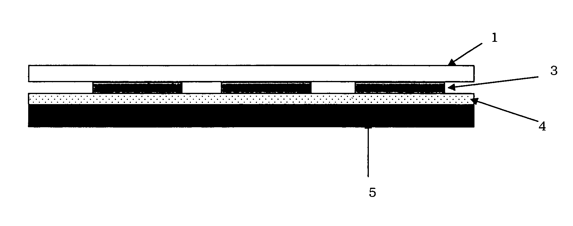
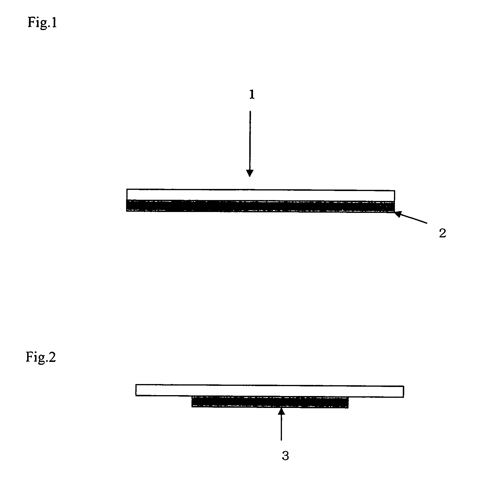
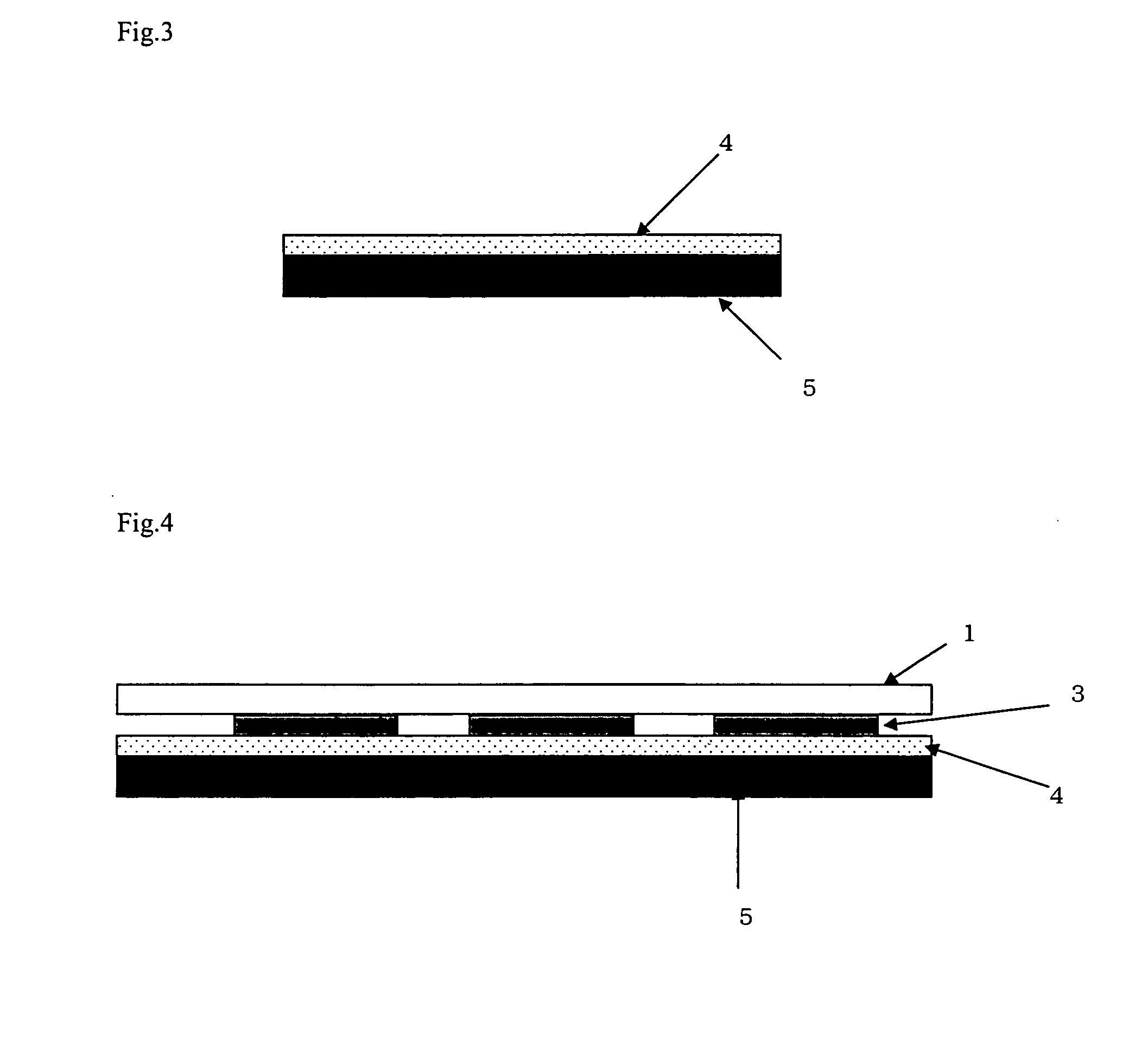
Image

Examples
examples
[0124]The present invention is now more specifically illustrated with reference to Examples. However, the present invention is not limited to these Examples.
[0125](Preparation Example of an Adhesive Layer (B))
synthesis example
[0126](I) Thermosetting Adhesive Component
[0127](I-1) Epoxy Compound (VG3101, manufactured by Mitsui Chemicals, Inc.)
[0128](I-2) Imidazole Type Hardener (2MAOK-PW, manufactured by Shikoku Chemicals Corporation)
[0129](II) Silica Type Filler (1-FX, manufactured by Tatsumori Co.)
[0130](III) Synthesis Example of Polyimide Resin Component
synthesis example 1
[0131]17.00 g of 4,4′-bis(3-aminophenoxy)biphenyl, 40.14 g of polytetramethyleneoxide-di-p-aminobenzoate (product name: Elasmer 1000, average molecular weight: 1,305, manufactured by Ihara Chemical Industry Co., Ltd.), 86.37 g of N-methyl-2-pyrrolidone and 37.09 g of mesitylene were measured and put into a 300-ml, 5-necked separable flask provided with a stirrer, a nitrogen gas inlet tube, a thermometer and a Dienstag tube filled with mesitylene. The resulting mixture was heated at 50° C. under a nitrogen atmosphere to dissolve, then 25.05 g of oxy-4,4′-diphthalate dianhydride was added in small portions. Then, the nitrogen gas inlet tube was inserted into the solution (in a bubbling state), and the solution was heated so that the temperature in the system is from 170 to 180° C. and retained for 10 hours while performing azeotropic removal of water. After cooling, 61.67 g of N-methyl-2-pyrrolidone and 26.49 g of mesitylene were added for diluting to obtain a solution of a polyimide ...
PUM
| Property | Measurement | Unit |
|---|---|---|
| Temperature | aaaaa | aaaaa |
| Angle | aaaaa | aaaaa |
| Percent by volume | aaaaa | aaaaa |
Abstract
Description
Claims
Application Information