High-energy radiation scintillation detector comprising multiple semiconductor slabs

Inactive Publication Date: 2008-08-14
KASTALSKY ALEXANDER +1
View PDF5 Cites 18 Cited by
  • Summary
  • Abstract
  • Description
  • Claims
  • Application Information

AI Technical Summary

Benefits of technology

[0010]To circumvent the problem of thickness limitation, arising from the finite absorption length for the scintillator light in the semiconductor slab, a new design is disclosed, according to the present invention, wherein the detector represents a multiple stack of relatively thin semiconductor slabs, each slab being thinner than the scintillator light absorption length. Each slab is further endowed with an epitaxially grown photo-detector that has high absorption coefficient for scintillator light and a sufficient thickness to fully absorb said scintillator light. The stack of such slabs according to the present invention can accommodate a long absorption length of the high-energy gamma radiation without any loss in either the scintillator yield or th

Problems solved by technology

Further increase of the electron density, desirable for the increase of the EF/kT ratio, becomes impractical due to the rise of the free-carrier absorpt

Method used


Image

  • High-energy radiation scintillation detector comprising multiple semiconductor slabs
  • High-energy radiation scintillation detector comprising multiple semiconductor slabs
  • High-energy radiation scintillation detector comprising multiple semiconductor slabs

Examples


Example

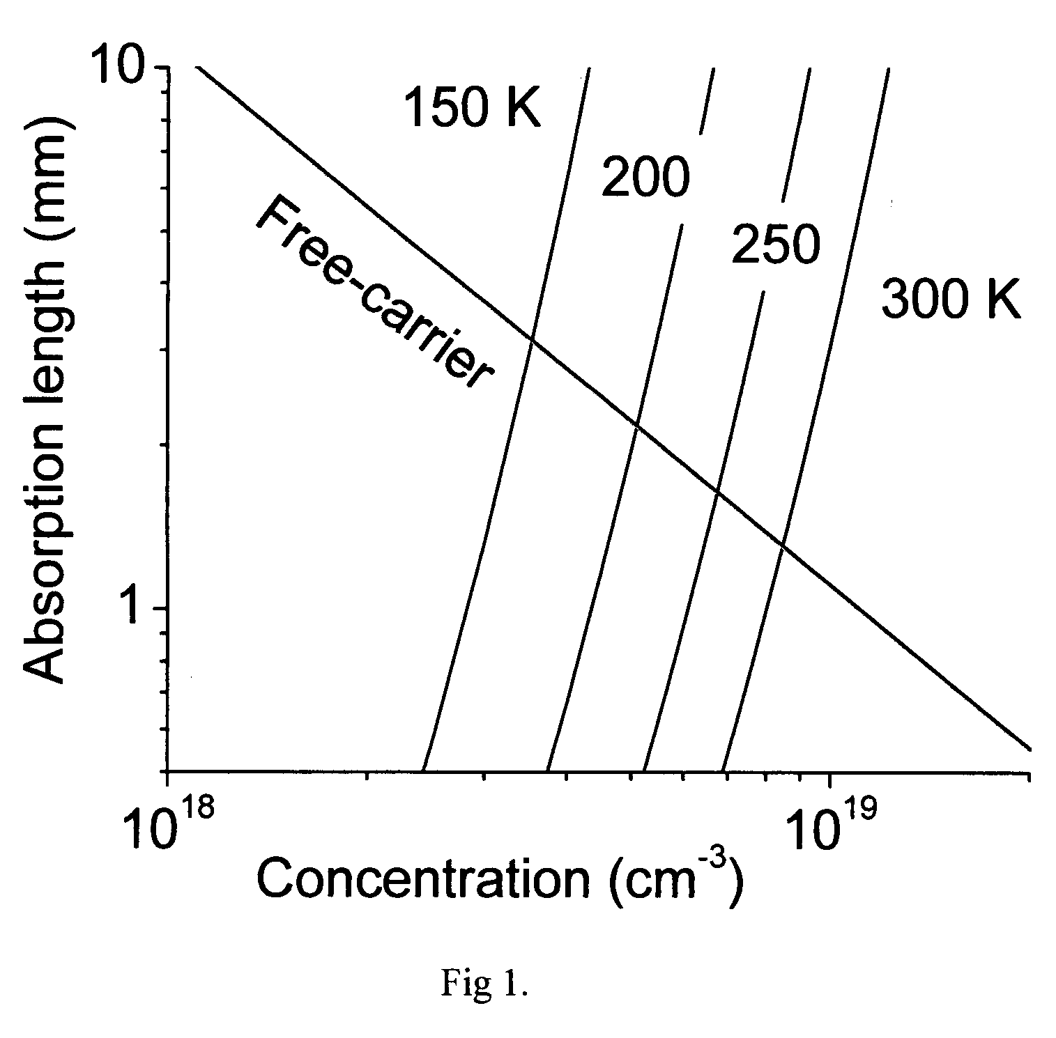
[0027]FIG. 1 shows the dependence of the absorption length λ on the electron concentration and temperature in n-type doped InP at the optical wavelength of 0.92 μm, typical for the InP interband emission spectrum. Both the interband and the free-carrier contributions to absorption are shown. The interband curves are labeled with the values of temperature T in degrees K. The free-carrier curve is approximately independent of temperature. Similar graphs, constructed for other than InP compound-semiconductor materials, like GaAs or CdTe, will serve to determine the maximum thickness L of semiconductor slabs according to the invention. In the preferred embodiment, one must have L<λ.

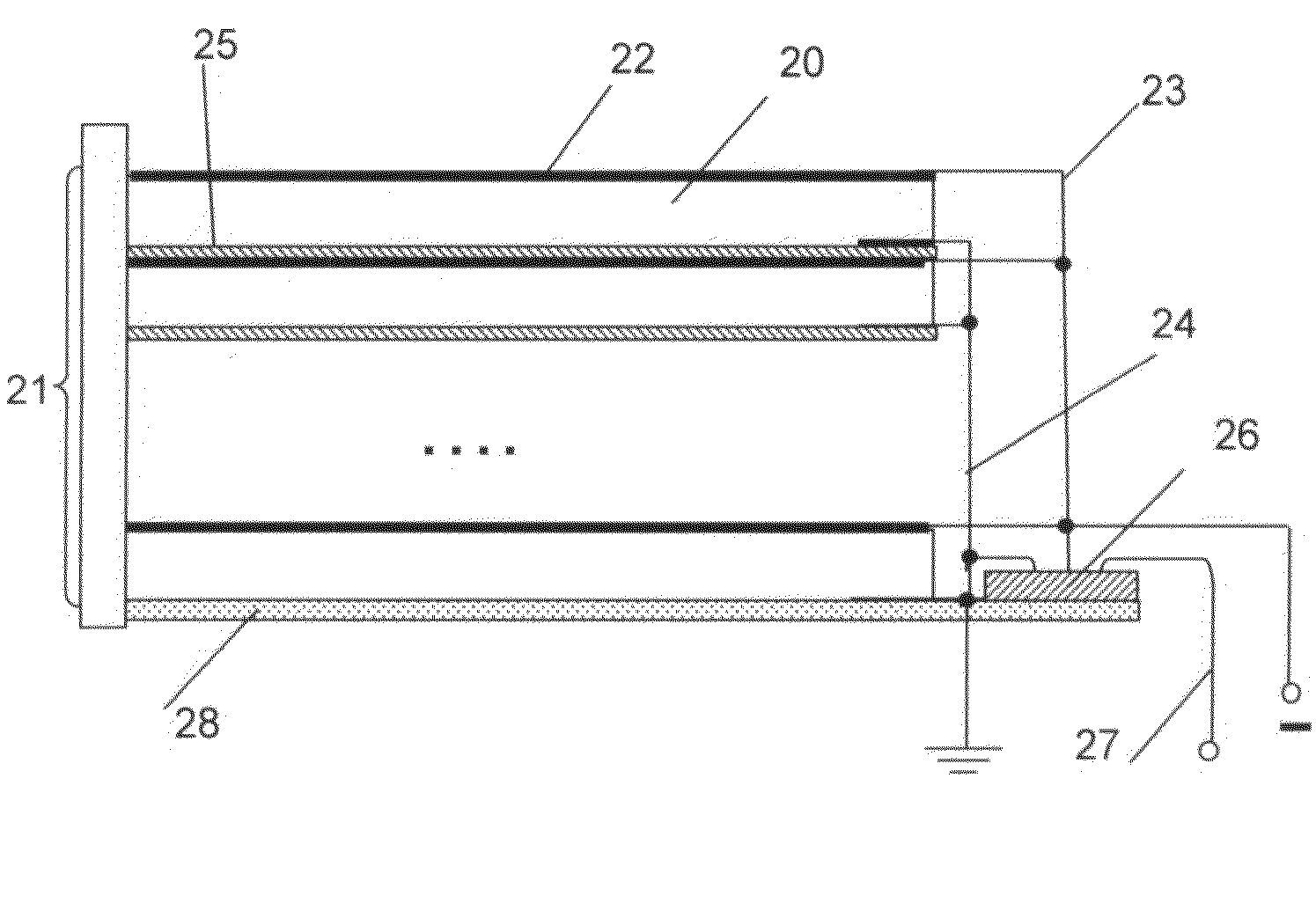
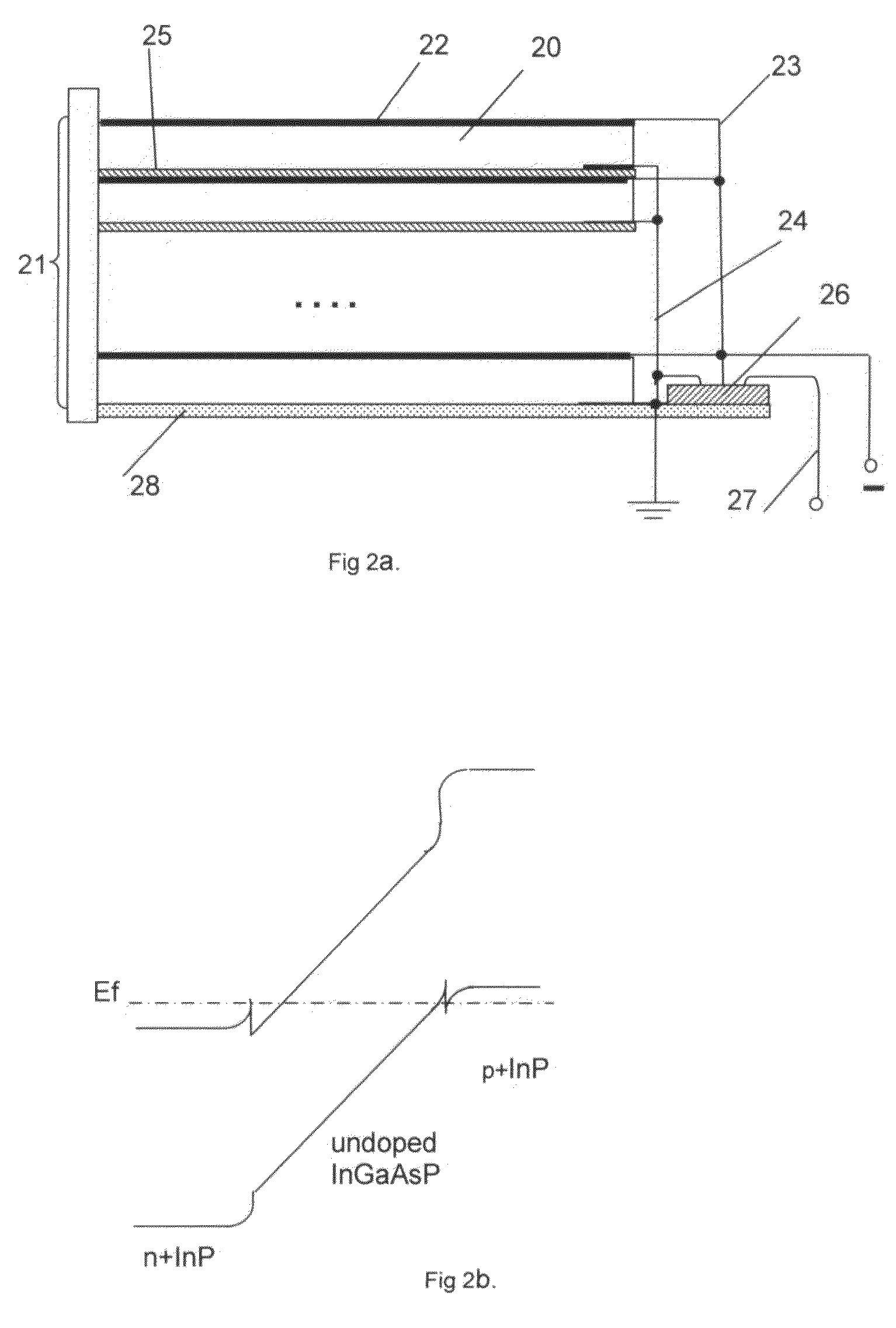
[0028]FIG. 2 schematically illustrates one of the embodiments of the non-pixellated radiation detector, according to the present invention. In FIG. 2a, a cross-sectional view of the device structure is presented. Multiple semiconductor slabs 20, are integrated into one block 21. The slabs 20 are isolated from...


PUM


Abstract

A multilayer semiconductor scintillator is disclosed for detection, energy quantification, and determination to source of high-energy radiation, such as gamma or X-ray photons or other particles that produce ionizing interaction in semiconductors. The basic embodiment of the inventive detector comprises a multiplicity of stacked direct-gap compound semiconductor wafers, such as InP and GaAs, each wafer heavily doped n-type so as to maximize its transparency to scintillating radiation. Each wafer is further endowed with surface means for detection of said scintillating radiation, such a hetero-epitaxial p-i-n photodiode. In a preferred embodiment, the photodiode layer in each wafer is pixellated so as to provide the x and y coordinates of an ionizing interaction event. Combined with the z coordinate provided by the wafer index in the stack, the inventive detector yields the three-dimensional coordinates of each ionizing interaction event associated with absorption of an individual quantum of high-energy radiation. This three-dimensional information enables a further disclosed advantageous analysis method that is suitable for rapid identification of radioactive isotopes and determination of the direction to the source of radiation.

Description

FIELD OF THE INVENTION[0001]The invention relates to solid-state high energy radiation detectors, more specifically to scintillating detectors made of direct-gap semiconductors.Introduction[0002]This patent application builds upon an earlier U.S. patent application Ser. No. 11 / 144,443, filed Jun. 6, 2005 and titled “Semiconductor scintillation high-energy radiation detector”. In that application, a semiconductor scintillator detector is disclosed in which ionizing radiation creates electron-hole pairs that subsequently undergo interband recombination, producing infrared light to be registered by a photo-detector. To make the semiconductor essentially transparent to its own interband radiation, a direct gap semiconductor, such as InP or GaAs, is heavily doped with shallow donors to produce the blue shift of the absorption edge, an effect known as the Burstein shift. Owing to the high Fermi level EF for electrons, in such materials the absorption edge is shifted to shorter wavelengths...

Claims


Application Information

Patent Timeline
IPC IPC(8): G01T1/20
CPCG01T1/2018G01T1/2928G01T1/20181
Inventor KASTALSKY, ALEXANDERLURYI, SERGE
Owner KASTALSKY ALEXANDER
Why Eureka
Try Eureka