Diode-Like Composite Semiconductor Device

a composite semiconductor and diode technology, applied in semiconductor devices, electronic switching, pulse techniques, etc., can solve the problems of low resistance strength of silicon sbd, inability to meet the requirements of low voltage, inability to meet the requirements of applications now under consideration, etc., and achieve the effect of minimal current capacity

Active Publication Date: 2008-08-14
SANKEN ELECTRIC CO LTD
View PDF1 Cites 128 Cited by
  • Summary
  • Abstract
  • Description
  • Claims
  • Application Information

AI Technical Summary

Benefits of technology

[0013]An additional advantage of the invention arises from the fact that the semiconductor rectifier and unipolar field effect transistor comprising the device of this invention are so made that the current flowing between the gate and second main electrode of the field effect transistor when this transistor is on is less then the current flowing between the first and the second electrode of the semiconductor rectifier. Consequently, the forward current of the device flows predominantly through the rectifier, hardly through the gate of the field effect transistor. The gate of the field effect transistor can therefore be of minimal current capacity.
[0014]The above and other objects, features and advantages of this invention will become more apparent, and the invention itself will best be understood, from a study of the following description and appended claims, with reference had to the attached drawings showing some preferable embodiments of the invention.

Problems solved by technology

A low-antivoltage-strength silicon SBD requires a relatively low forward voltage (curve B in FIG. 4A) but is incapable of withstanding as high a voltage as required in the applications now under consideration.
It might be contemplated to design these SBDs for a low forward voltage drop, but then they would also in inconveniently low in withstanding capability due to a rise in current leakage in response to a reverse voltage.

Method used


Image

  • Diode-Like Composite Semiconductor Device
  • Diode-Like Composite Semiconductor Device
  • Diode-Like Composite Semiconductor Device

Examples


embodiment

of FIG. 7

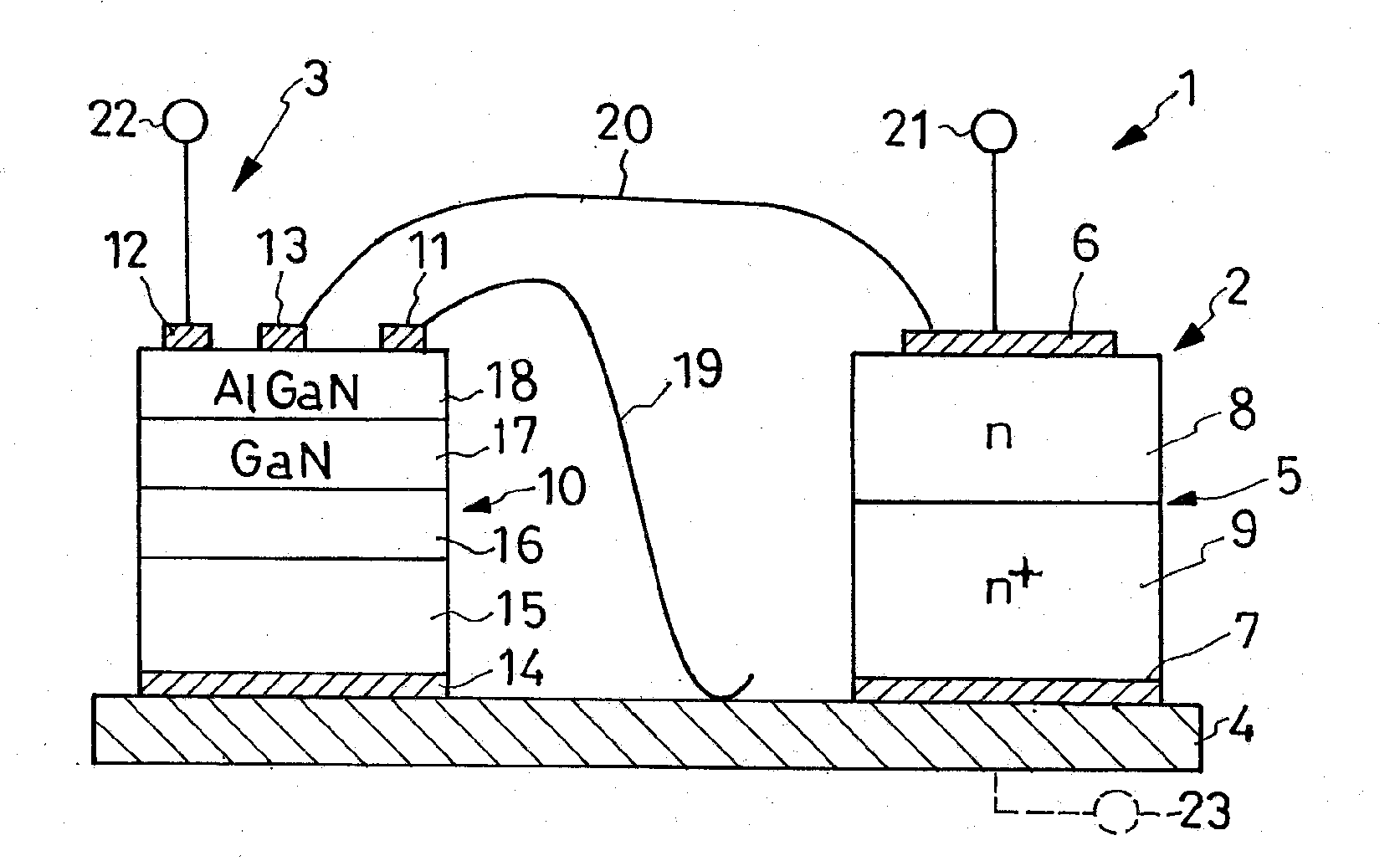
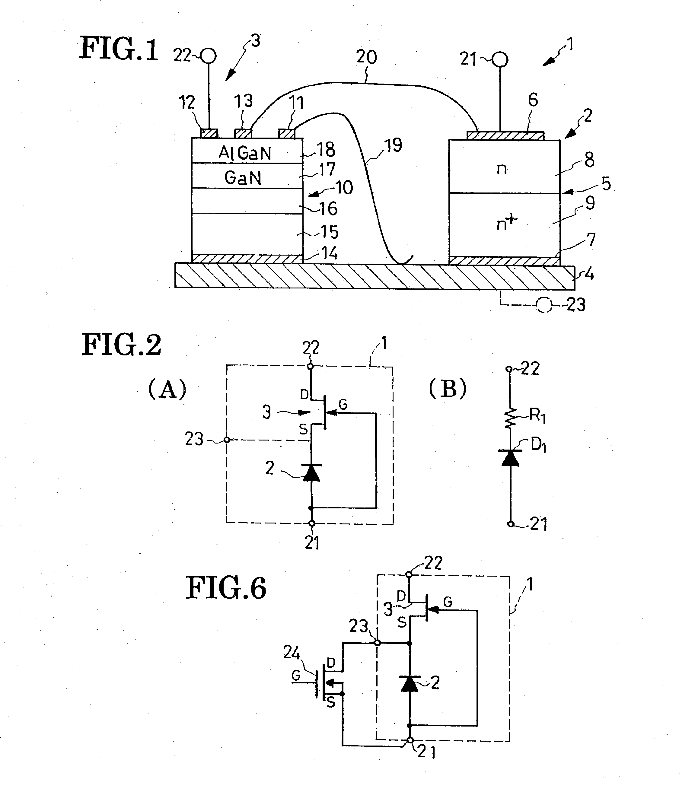
[0066]This second preferred form of composite semiconductor device 1a features a Si pn-junction diode 2a employed in lieu of the Si SBD 2, FIG. 1, of the first described composite semiconductor device 1. All the other details of construction of this device 1a are as previously set forth in connection with the first described device 1.

[0067]The Si pn-junction diode 2a of the second composite semiconductor device 1a has a body 5a of doped silicon between an anode or first electrode 6a and a cathode or second electrode 7a. The silicon body 5a is a lamination of a first semiconductor layer shown as a p+-type semiconductor layer 31, a second semiconductor layer shown as an n-type semiconductor layer 32, and a third semiconductor layer shown as an n+-type semiconductor layer 33, arranged in that order from anode 6a toward cathode 7a. The n-type semiconductor layer 32 is less in n-type impurity concentration than the n+-type semiconductor layer 33. Alternatively, an intrinsic semi...


PUM


Abstract

A silicon-made low-forward-voltage Schottky barrier diode is serially combined with a high-antivoltage-strength high-electron-mobility transistor made from a nitride semiconductor that is wider in bandgap than silicon. The Schottky barrier diode has its anode connected to the gate, and its cathode to the source, of the HEMT. This HEMT is normally on. The reverse voltage withstanding capability of the complete device depends upon that between the drain and gate of the HEMT.

Description

CROSS REFERENCE TO RELATED APPLICATIONS[0001]This application claims priority to Japanese Patent Application No. 2007-031103, filed Feb. 9, 2007.BACKGROUND OF THE INVENTION[0002]This invention relates to composite semiconductor devices, particularly to one integrally comprising a semiconductor rectifier and unipolar field effect transistor, altogether functioning as diode. More particularly, the invention is directed to such a diode-like semiconductor device which has an improved recovery time, antivoltage strength, and forward voltage requirement.[0003]Inverters (DC-to-AC converters) and switching-mode power supplies are alike in incorporating a switching device that rapidly turns on and off. The voltage applied to the switching devices for their on-off control is so high that the diodes put to combined use therewith must necessarily have a correspondingly high antivoltage strength and short reverse recovery time. These requirements are met to some extent by the known silicon pin (...

Claims


Application Information

Patent Timeline
Patent Type & Authority Applications(United States)
IPC IPC(8): H01L27/06
CPCH01L25/18H01L2924/12032H03K17/567H03K17/74H01L2224/48137H01L2224/73265H01L2224/32145H01L2224/32245H01L2224/48247H01L27/0605H01L2924/13055H01L2924/13091H01L29/2003H01L29/7786H01L29/4175H01L2924/1305H01L2924/13062H01L2924/30107H01L2924/00H01L2224/48257
Inventor MACHIDA, OSAMUIWABUCHI, AKIO
Owner SANKEN ELECTRIC CO LTD
Why Eureka
Try Eureka