Integrated mosfet and schottky device

a mosfet and schottky technology, applied in semiconductor devices, diodes, electrical apparatus, etc., can solve the problems that the tmbs type device may not be suitable for a mosfet and schottky device integrated technology, and the tmbs type device may not meet the requirements of the tmbs type device. , to achieve the effect of low leakage, low vf and high leakag

Active Publication Date: 2008-08-14
INFINEON TECH AMERICAS CORP
View PDF6 Cites 12 Cited by
  • Summary
  • Abstract
  • Description
  • Claims
  • Application Information

AI Technical Summary

Benefits of technology

[0004]According to one aspect of the present invention, a high performance Schottky diode is integrated with a MOSFET having deep source field electrodes. Advantageously, the deep source field electrodes of the MOSFET allow an integrated Schottky with low reverse leakage and low Vf to be formed when the mesa width is appropriately chosen.
[0005]Simulations have shown that a Schottky diode in a device according to the present invention offers both lower leakage and Vf than a Schottky diode that could be created with a traditional trench process flow. Moreover, such a device may exhibit significantly lower Vf than a MOSFET integrated with a pn junction diode which allows a Schottky diode according to the present invention to operate at higher current levels.

Problems solved by technology

Current trench technologies for devices with higher breakdown voltages (40-300) may not be suitable for an integrated TMBS type device due to higher leakage and Vf.

Method used


Image

  • Integrated mosfet and schottky device
  • Integrated mosfet and schottky device
  • Integrated mosfet and schottky device

Examples


first embodiment

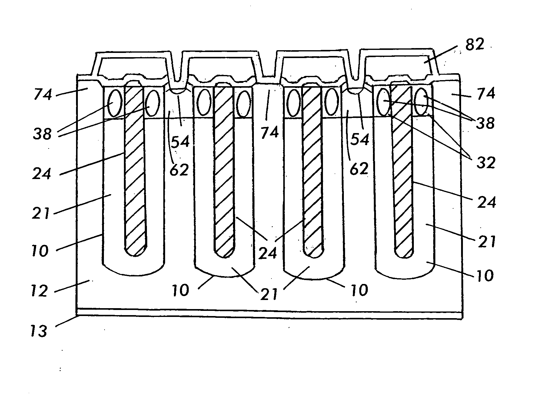
[0011]Referring to FIG. 1, a semiconductor device according to the present invention is preferably a power MOSFET that includes a plurality of spaced deep source trenches 10 formed in a semiconductor body 12, which can be an epitaxially grown silicon body of one conductivity (e.g. N type) disposed over a silicon substrate 13 of the same conductivity. Each trench 10 includes a thick oxide body 21 disposed in the interior and lining at least the bottom and a portion of the sidewalls thereof. A device according to the present invention further includes base regions 62 of the opposite conductivity to body 12 (e.g. P type), source regions 60 of the same conductivity as body 12 formed in base regions 62, a plurality of insulated gate electrodes 38 each insulated from a respective base region 62 by a gate oxide body 32, which is thinner than thick oxide body 21, disposed in trenches 10, a plurality of deep source electrodes 24 which are insulated from, but extend through respective pairs o...

second embodiment

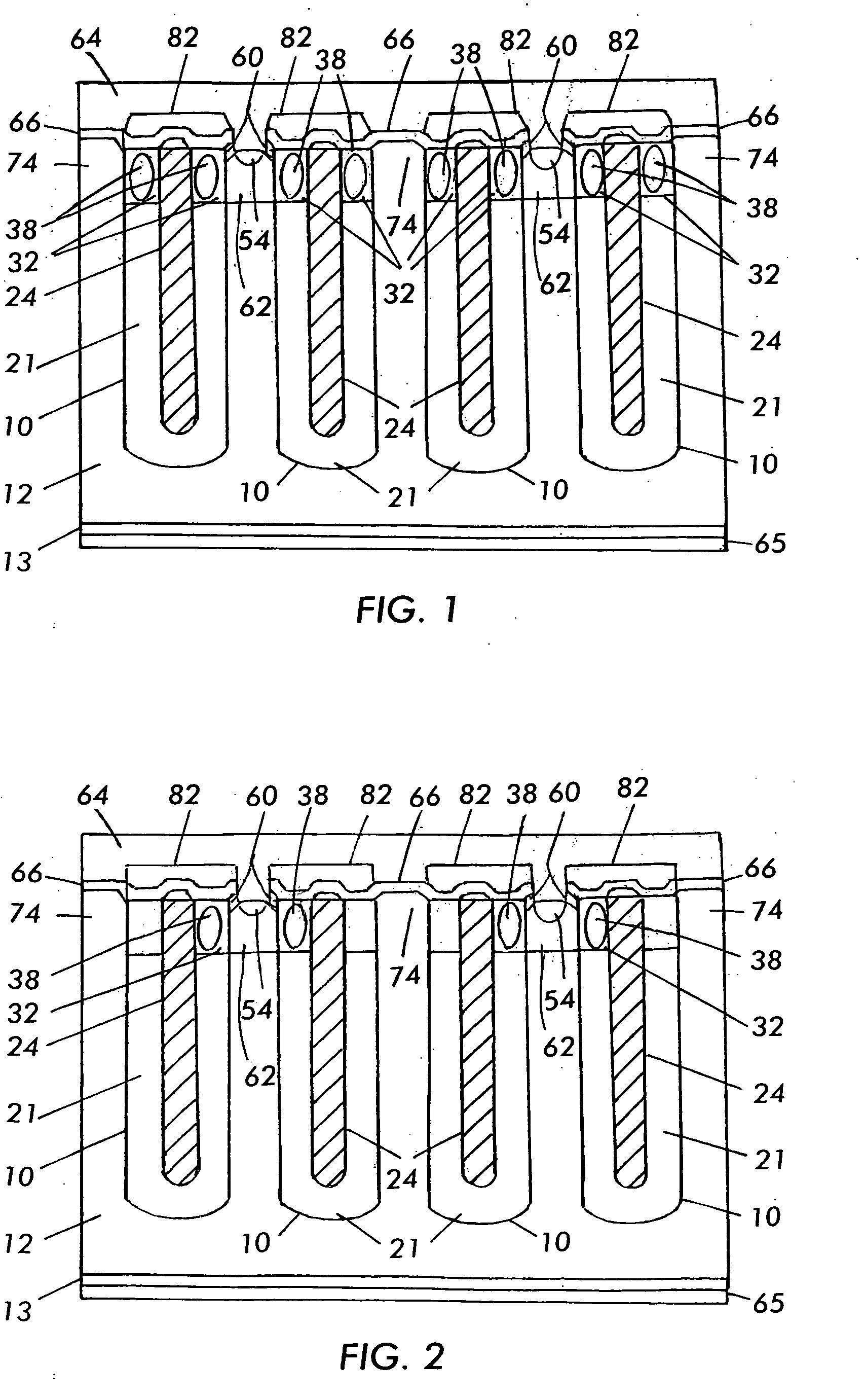
[0016]A device may be useful in cases involving high electric field across the gate oxide.

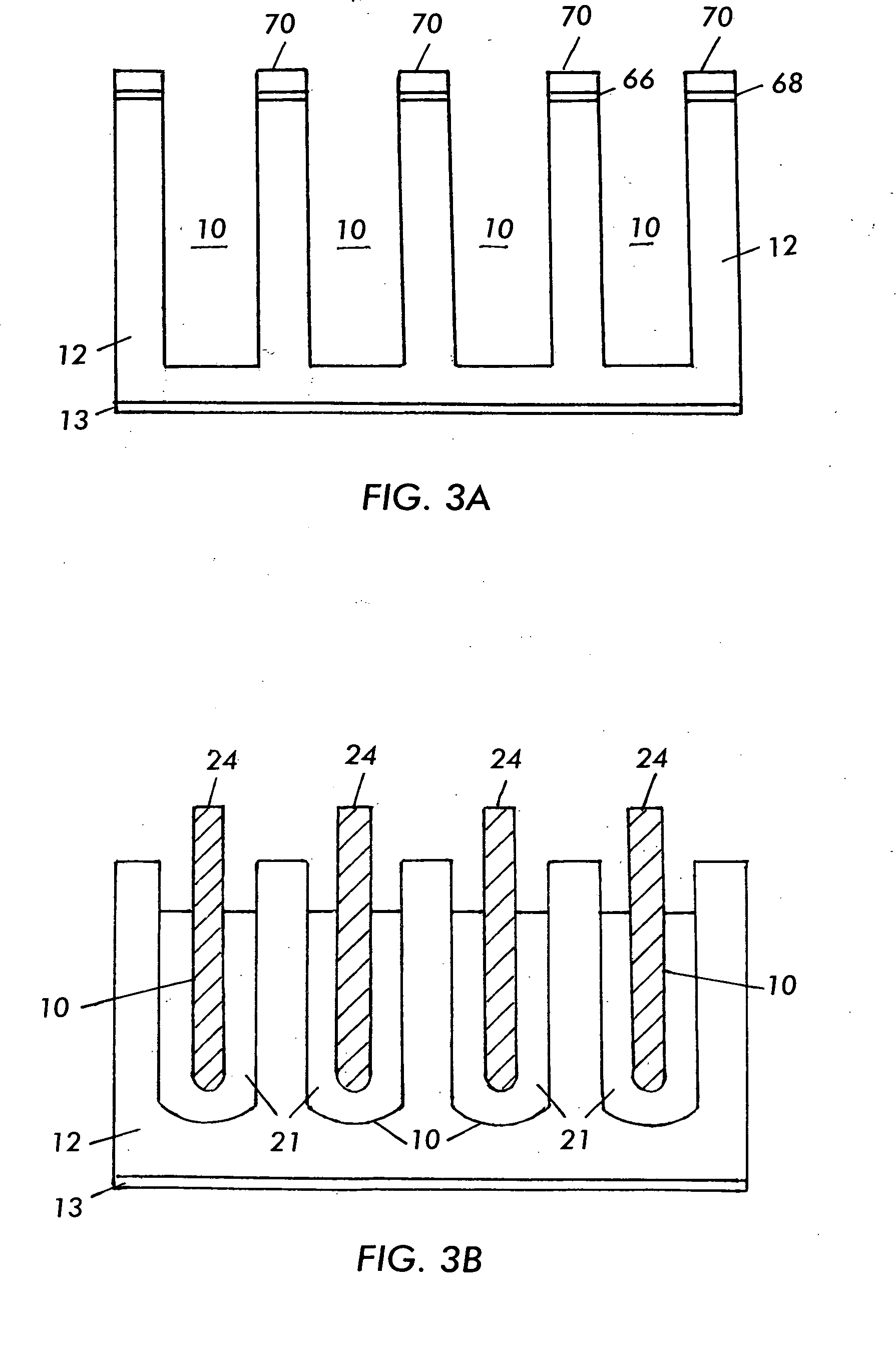
[0017]Referring now to FIG. 3A, to fabricate a device according to the present invention, pad oxide 68 is grown over a surface of semiconductor body 12, a nitride hard mask 70 is deposited over pad oxide 68, and a plurality of source trenches 10 are formed in semiconductor body 12 by etching pad oxide 68 and silicon from the bottom of openings in mask 70.

[0018]Referring next to FIG. 3B, thick oxide 21 is grown inside trenches 10 using any desired method. For example, a method as set forth in U.S. application Ser. No. 11 / 890,849 can be used to form thick oxide 21. The same method can be used to obtain source field electrode 24 as illustrated by FIG. 3B. Namely, field electrodes that extend above the top surface of thick oxide bodies 21.

[0019]Referring next to FIG. 3C, gate oxide 32 is grown on the exposed surfaces of the mesas between trenches 10 in an oxidation process which also oxidizes the ...


PUM


Abstract

A power semiconductor device that includes a trench power MOSFET with deep source field electrodes and an integrated Schottky diode.

Description

RELATED APPLICATION[0001]This application is based on and claims priority to U.S. Provisional Application Ser. No. 60 / 900,252, filed on Feb. 8, 2007, entitled Deep Trench Schottky Device, to which a claim of priority is hereby made and the disclosure of which is incorporated by reference.BACKGROUND AND SUMMARY OF THE INVENTION[0002]US Patent application published as US Patent Publication No. 2006 / 0033154 and U.S. patent application Ser. No. 11 / 890,849 both assigned to the assignee of the present application and incorporated by reference, disclose power MOSFETs having deep source field electrodes.[0003]Integrated Schottky diodes are available in state of the art trench MOSFETs with breakdown voltages in the range of 20-30V. These Schottky diodes take advantage of the trench structure to form a Trench MOS Barrier Schottky (TMBS) structure that provides low leakage and low Vf compared to planar Schottky diodes. Current trench technologies for devices with higher breakdown voltages (40-...

Claims


Application Information

Patent Timeline
Patent Type & Authority Applications(United States)
IPC IPC(8): H01L29/78
CPCH01L29/407H01L29/41766H01L29/42368H01L29/7813H01L29/66727H01L29/66734H01L29/7806H01L29/456
Inventor HENSON, TIMOTHYGIRDHAR, DEV ALOK
Owner INFINEON TECH AMERICAS CORP
Why Eureka
Try Eureka