Method for Manufacturing Passive Device and Semiconductor Package Using Thin Metal Piece

a technology of passive devices and semiconductor packages, which is applied in the direction of solid-state devices, transportation and packaging, basic electric elements, etc., can solve the problem of not effectively transferring heat from the devices to the surface of the substrate, and achieve the effects of reducing manufacturing time and cost, high electrical conductivity, and high quality

Inactive Publication Date: 2008-08-14
WAVENICS +1
View PDF9 Cites 17 Cited by
  • Summary
  • Abstract
  • Description
  • Claims
  • Application Information

AI Technical Summary

Benefits of technology

[0014]Accordingly, the present invention is directed to a method for manufacturing passive devices and semiconductor packages using a thin metal piece capable of providing high quality passive devices having high electrical conductivity and reducing manufacturing time and costs by selectively etching and polishing the thin metal piece to simultaneously form passive devices such as high quality inductors and vias using a semiconductor process.

Problems solved by technology

The related art semiconductor package for heat emission can improve an heat-emission effect more or less using the metal cap, but substrates such as PCBs on which passive devices (inductors, capacitors, resistors, transmission lines), passive circuits, semiconductors are mounted are plastic substrates or ceramic substrates having low thermal conductivity, so that such substrates have a problem of not effectively emitting heat transferred from the devices to the surface of the substrate.

Method used


Image

  • Method for Manufacturing Passive Device and Semiconductor Package Using Thin Metal Piece
  • Method for Manufacturing Passive Device and Semiconductor Package Using Thin Metal Piece
  • Method for Manufacturing Passive Device and Semiconductor Package Using Thin Metal Piece

Examples


first embodiment

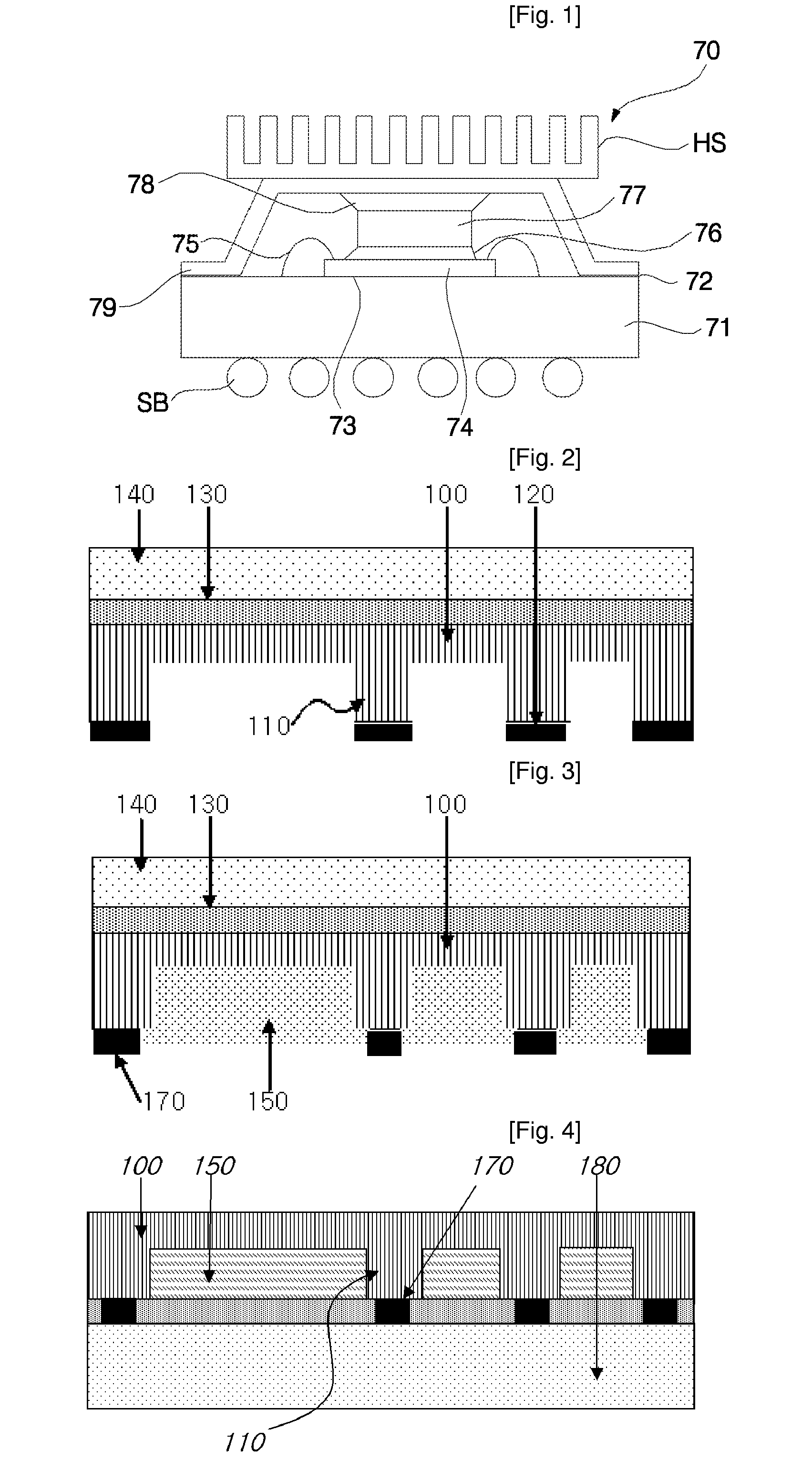
[0029]FIGS. 2 to 5 are views illustrating processes for forming passive devices using a thin metal piece according to the present invention.

[0030]First, a thin metal piece 100 is boned on a backside of a dummy substrate 140 having excellent flatness using an adhesive layer 130. Masking material 120 such as SiO2 or SiNx is attached on a backside of the thin metal piece 100, regions where vias 110 are to be formed are patterned, the backside of the thin metal piece 100 is etched at a predetermined depth. At this point, the etching may be performed using a chemical etching.

[0031]Next, the masking material 120 is removed and a polymer layer 150 made of a material such as benzocyclobutene (BCB), polyimide (PI), bismaleimide triazine (BT) is formed on the entire backside of the thin metal piece.

[0032]After that, referring to FIG. 3, the polymer layer 150 below the regions where the vias 110 are to be formed is removed using a photolithography and metal pads 170 are formed. The formed devi...

second embodiment

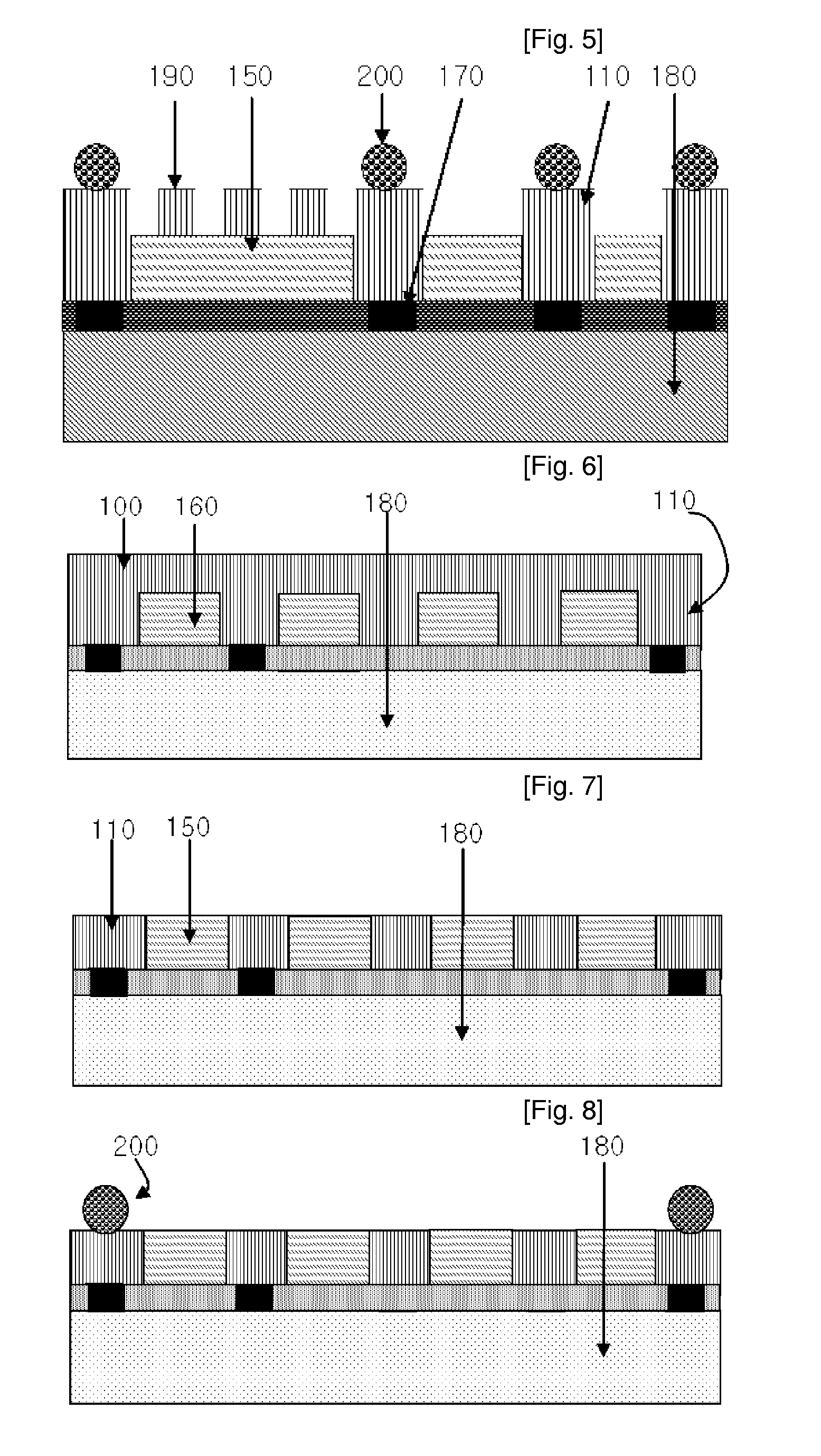
[0035]FIGS. 6 to 8 are views illustrating processes for forming passive devices using a thin metal piece according to the present invention.

[0036]First, a thin metal piece 100 is bonded on a backside of a dummy substrate 140 having excellent flatness using an adhesive layer 130 as in FIG. 2 illustrating the first embodiment. With a masking material 120 such as SiO2 and SiNx attached on a backside of the thin metal piece 100, regions where insulators 160 are to be formed are patterned. After that, the insulators 160 are formed at a predetermined depth in required regions of the thin metal piece 100 as illustrated in FIG. 6. At this point, an ion implantation or an anodization is used so as to form the insulators 160 in the required regions.

[0037]When the formed devices are attached on a lower substrate such as an IPD and an IC chip and the adhesive layer 130 and the dummy substrate 140 having excellent flatness are removed, a shape illustrated in FIG. 6 can be obtained.

[0038]Now, des...

third embodiment

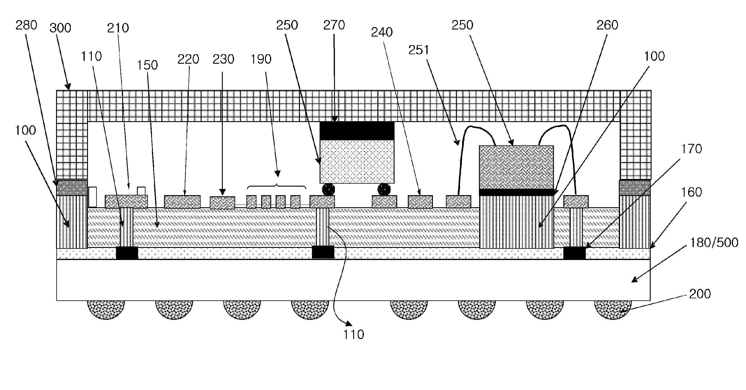
[0040]FIG. 9 is a sectional view of passive devices that uses a thin metal piece according to the present invention.

[0041]In FIG. 9, after inductors 190 and vias 110 are selectively formed on the thin metal piece 100 by the processes illustrated in FIGS. 2 to 5, passive devices are manufactured on a polymer layer 150 or a metal surface. Referring to FIG. 9, passive devices such as a transmission line 210, a capacitor 220, a resistor 230 are formed on the polymer layer 150 using a semiconductor manufacturing process. A capacitor 240 can be also directly manufactured on the exposed metal surface using the anodization method.

[0042]Through these processes, inductors 190 and vias 110 of high quality can be easily formed on the thin metal piece 100. The thin metal piece where the passive devices are integrated can be connected with and stacked on another thin metal piece, another IPD, or RF (radio frequency) chip (not shown) using an interconnection via 110.


PUM

PropertyMeasurementUnit
depthaaaaaaaaaa
flatnessaaaaaaaaaa
thickaaaaaaaaaa

Abstract

A method for manufacturing passive devices and semiconductor packages using a thin metal piece is provided. According to the method, an adhesive layer is formed on a dummy substrate; a thin metal piece is bonded on the adhesive layer; a masking material is attached to the thin metal piece, a region where vias are to be formed is patterned, the thin metal piece is etched at a predetermined depth; the masking material is removed, the etched portion is filled with polymer to form a flat polymer layer, a masking material is attached on the polymer layer, a region that is to be attached to an IPD or an IC chip is patterned, a metal pad is formed, and the formed devices are attached to a lower substrate using the metal pad; the adhesive layer and the dummy substrate are removed, a masking material is attached on a surface exposed, a region where passive devices are to be formed is patterned, and the thin metal piece is etched at a predetermined depth; and solder bumps for surface mounting are formed.

Description

BACKGROUND OF THE INVENTION[0001]1. Field of the Invention[0002]The present invention relates to a method for manufacturing passive devices and packages using a thin metal piece, and more particularly, to a method for manufacturing passive devices and semiconductor packages capable of manufacturing passive devices required for a system construction on a polymer layer, effectively emitting heat by attaching semiconductor devices in a bare-chip state on a thin metal piece using a flip-chip bonding or a wire-bonding, and selectively integrating the passive devices having excellent electrical property even in ultrahigh frequency waves on the polymer layer.[0003]2. Description of the Related Art[0004]Generally, one of important properties required for a semiconductor package is a heat emission property. Particularly, as semiconductor devices are high-speed and high-power oriented recently, much researches and developments are being carried out so as to deal with high heat generation.[000...

Claims


Application Information

Patent Timeline
Patent Type & Authority Applications(United States)
IPC IPC(8): H01L21/00
CPCH01L21/4846H01L21/486H01L2224/16225H01L21/6835H01L23/49816H01L23/49822H01L23/49827H01L23/5227H01L23/66H01L2221/68363H01L2224/32188H01L2224/48227H01L2224/73253H01L2224/92247H01L2924/01013H01L2924/01015H01L2924/01029H01L2924/01051H01L2924/01078H01L2924/01079H01L2924/01082H01L2924/07802H01L2924/14H01L2924/15311H01L2924/16152H01L2924/19011H01L2924/19041H01L2924/19042H01L2924/19043H01L24/32H01L24/48H01L2924/01033H01L2924/00011H01L2924/00014H01L2924/15787H01L2924/181H01L2924/00H01L2224/0401H01L2224/45099H01L2224/45015H01L2924/207H01H15/10H01H2231/026
Inventor KWON, YOUNG-SEKIM, KYOUNG-MIN
Owner WAVENICS
Why Eureka
Try Eureka