Method of manufacturing a semiconductor integrated circuit device

a manufacturing technology and integrated circuit technology, applied in semiconductor/solid-state device testing/measurement, manufacturing tools, instruments, etc., can solve the problems of difficult to efficiently shrink a chip, difficult to allocate probes, and difficulty in adjusting so as to improve the manufacturing yield of the semiconductor integrated circuit device. , the effect of reducing the operating rate of the probe testing apparatus

Inactive Publication Date: 2008-08-21
RENESAS ELECTRONICS CORP
View PDF4 Cites 16 Cited by
  • Summary
  • Abstract
  • Description
  • Claims
  • Application Information

AI Technical Summary

Benefits of technology

[0019]It is possible to improve a manufacturing yield of a semiconductor integrated circuit device.
[0020]Also, it is possible to prevent a membrane probe and a wafer to be tested from being broken, in a probe testing using a membrane probe with probes formed by a manufacturing technology of a semiconductor integrated circuit device.
[0021]Also, probe testing can be performed without decreasing operating rates of a probe testing apparatus.

Problems solved by technology

Along with such a narrower pitch of test pads, there has arisen a problem that it is difficult to allocate probes so as to fit test pad arrangement positions, when a prober with cantilever type probes is used for a probe testing.
The problem that a testing technology cannot follow a narrower pitch of pads is extremely serious.
That is, it becomes difficult to shrink a whole chip efficiently because of the difficulty of realizing a narrower pad pitch, even if it becomes possible to shrink an integrated circuit portion by micro-fabrication of semiconductor elements, which is realized by improvements of semiconductor chip manufacturing technologies such as photo-lithography and etching technology.

Method used


Image

  • Method of manufacturing a semiconductor integrated circuit device
  • Method of manufacturing a semiconductor integrated circuit device
  • Method of manufacturing a semiconductor integrated circuit device

Examples


Embodiment Construction

[0050]Before describing the present invention in detail, meanings of terms in the present application will be described as follows.

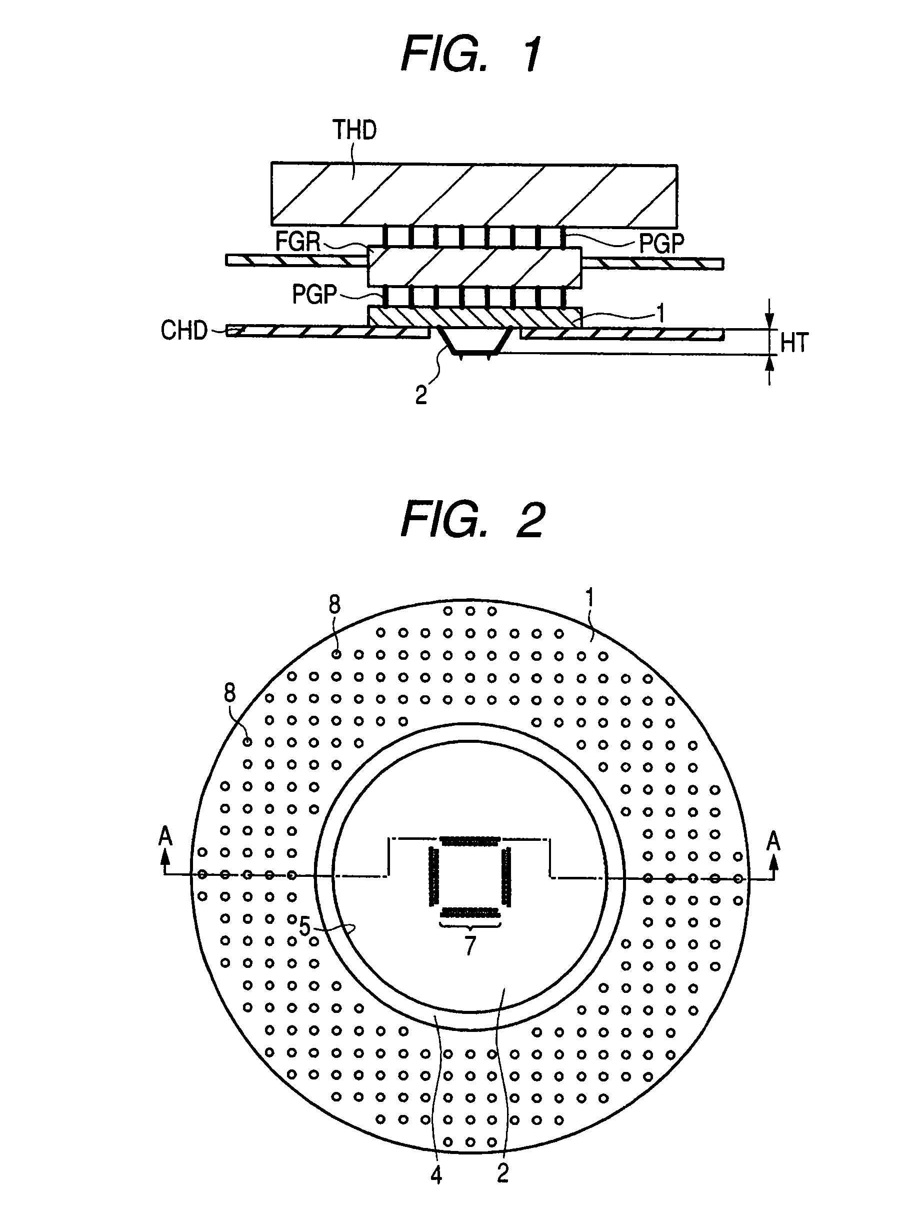
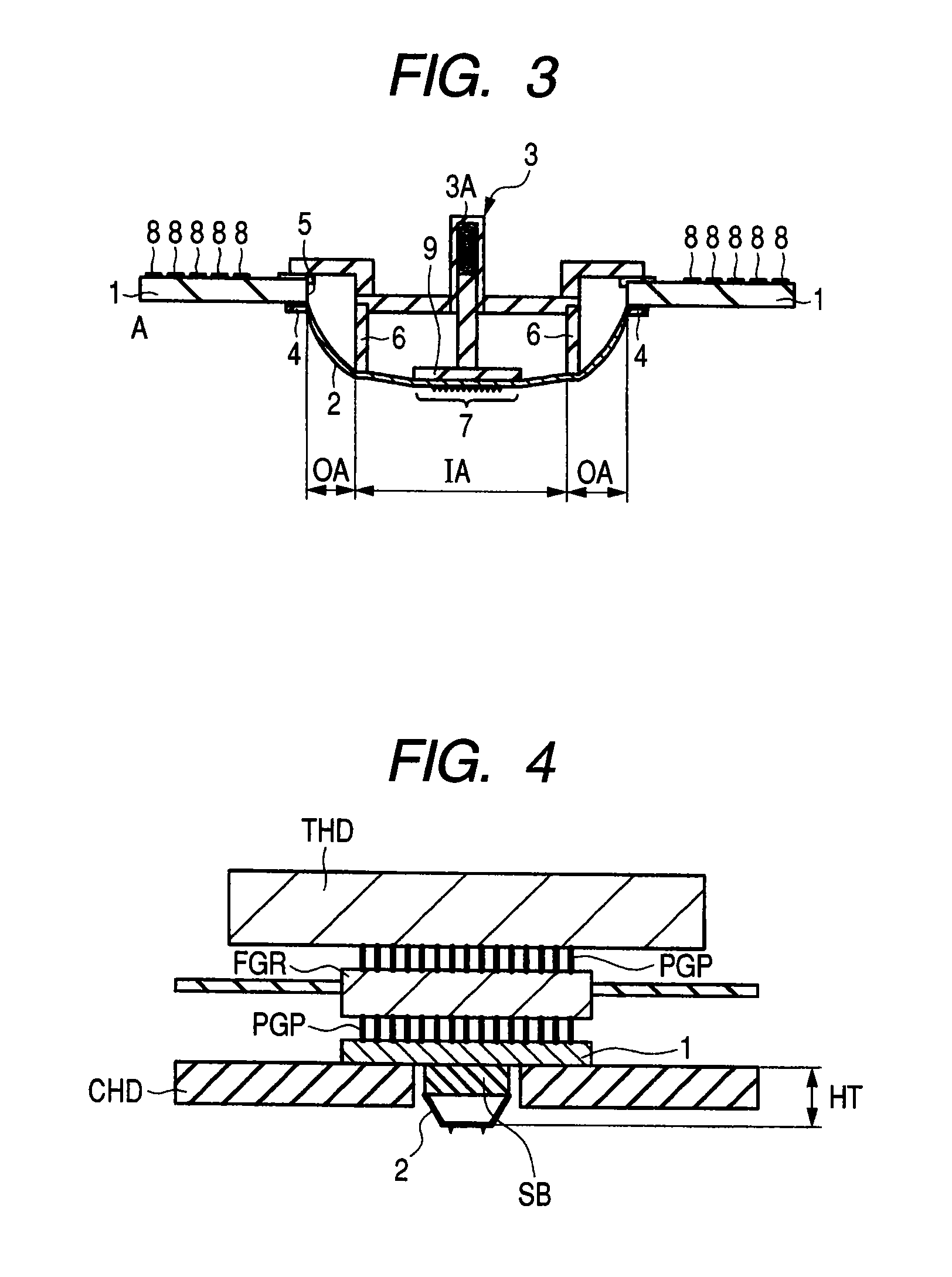
[0051]A device surface means a main surface of a wafer on which device patterns corresponding to a plurality of chip regions are formed.

[0052]A contact terminal or probe means a stylus, probe needle, protrusion or the like for performing a testing of electric characteristics by being brought into contact with electrode pads provided over each chip region.

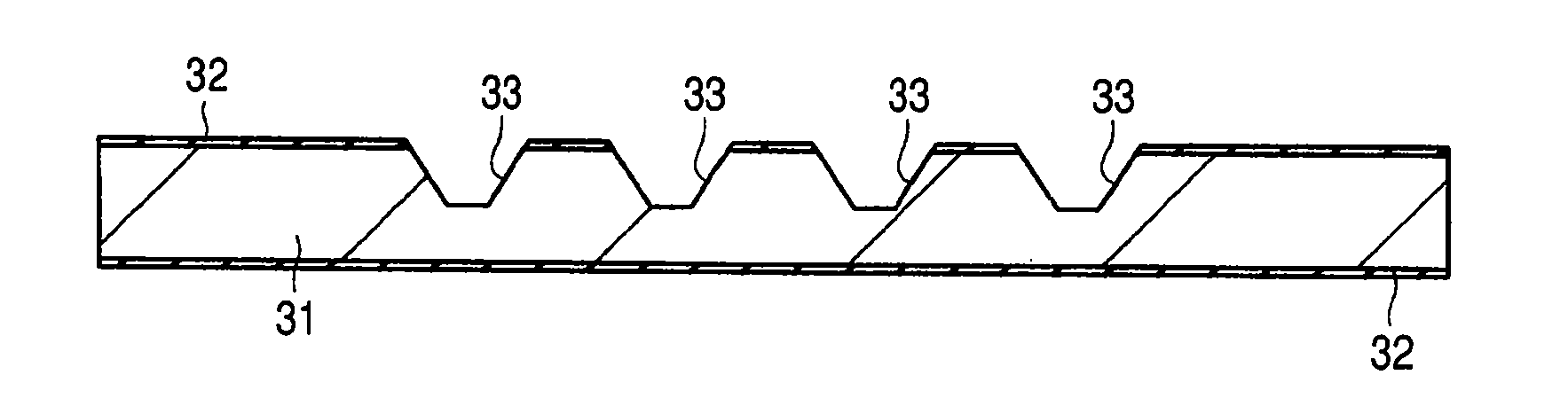
[0053]A membrane probe, membrane probe-card or protruded-stylus wiring sheet composite means a membrane which is provided with the contact terminals (protruded styluses) contacting an object to be tested as mentioned above and wires drawn and extended therefrom over which electrodes for outside contacts are formed, a membrane which is 10 to 100 μm, for example, in thickness, and a membrane on which a wire layer and tips (contact terminals) electrically coupled therewith are formed in an integrated manner...


PUM


Abstract

An object is to prevent a breakage of a membrane probe and a wafer to be tested in a probe testing using a membrane probe with styluses formed by a manufacturing technology for a semiconductor integrated circuit device.
Measures are: obtaining an image of a region PCA within the surface of a wafer including a region OGA pressed by a pressing member, at the center of which a chip just after probe-tested is located, by an imaging means such as a camera; comparing an image of a normal chip obtained in advance and an image of all the chips within the region PCA; and judging thereby whether an abnormal shape is caused or not in all the chips within the region PCA.

Description

CROSS-REFERENCE TO RELATED APPLICATION[0001]The disclosure of Japanese Patent Application No. 2007-36918 filed on Feb. 16, 2007 including the specification, drawings and abstract is incorporated herein by reference in its entirety.BACKGROUND OF THE INVENTION[0002]The present invention relates to manufacturing technology for a semiconductor integrated circuit device, and particularly to a technology effectively applied to an electrical testing of a semiconductor integrated circuit device, wherein probes of a probe-card are pressed onto electrode pads of the semiconductor integrated circuit device.[0003]Regarding probing of a semiconductor chip with bump electrodes of a semiconductor wafer, Japanese patent laid-open No. 2006-49599 discloses technology wherein an image of a state on each bump electrode is captured by a camera just after contact thereof with each probe, and a peripheral shape of each bump electrode (whether deformed or not), foreign material (bump chips) generation betw...

Claims


Application Information

Patent Timeline
Patent Type & Authority Applications(United States)
IPC IPC(8): H01L21/66
CPCG01R1/0483G01R35/00H01L2224/16H01L2924/014H01L22/14H01L2924/00011H01L2924/00014H01L2224/0401B24C3/083B24C3/12B24C9/00
Inventor OKAYAMA, MASAO
Owner RENESAS ELECTRONICS CORP
Why Eureka
Try Eureka