Switching Device

Inactive Publication Date: 2008-08-28
ELEMENT SIX LTD
View PDF4 Cites 33 Cited by
  • Summary
  • Abstract
  • Description
  • Claims
  • Application Information

AI Technical Summary

Problems solved by technology

All practical switching materials and devices fall short of this ideal, and an area of particular difficulty is in switches required to withstand both high voltages in the ‘off’ state and high currents in the ‘on’ state.
Using silicon for such a switch would involve excessively large voltage blocking layers, which may not be realistically possible (especially if reverse voltages in excess of 10 kV are involved), as this will lead t

Method used


Image

  • Switching Device
  • Switching Device
  • Switching Device

Examples


example 1

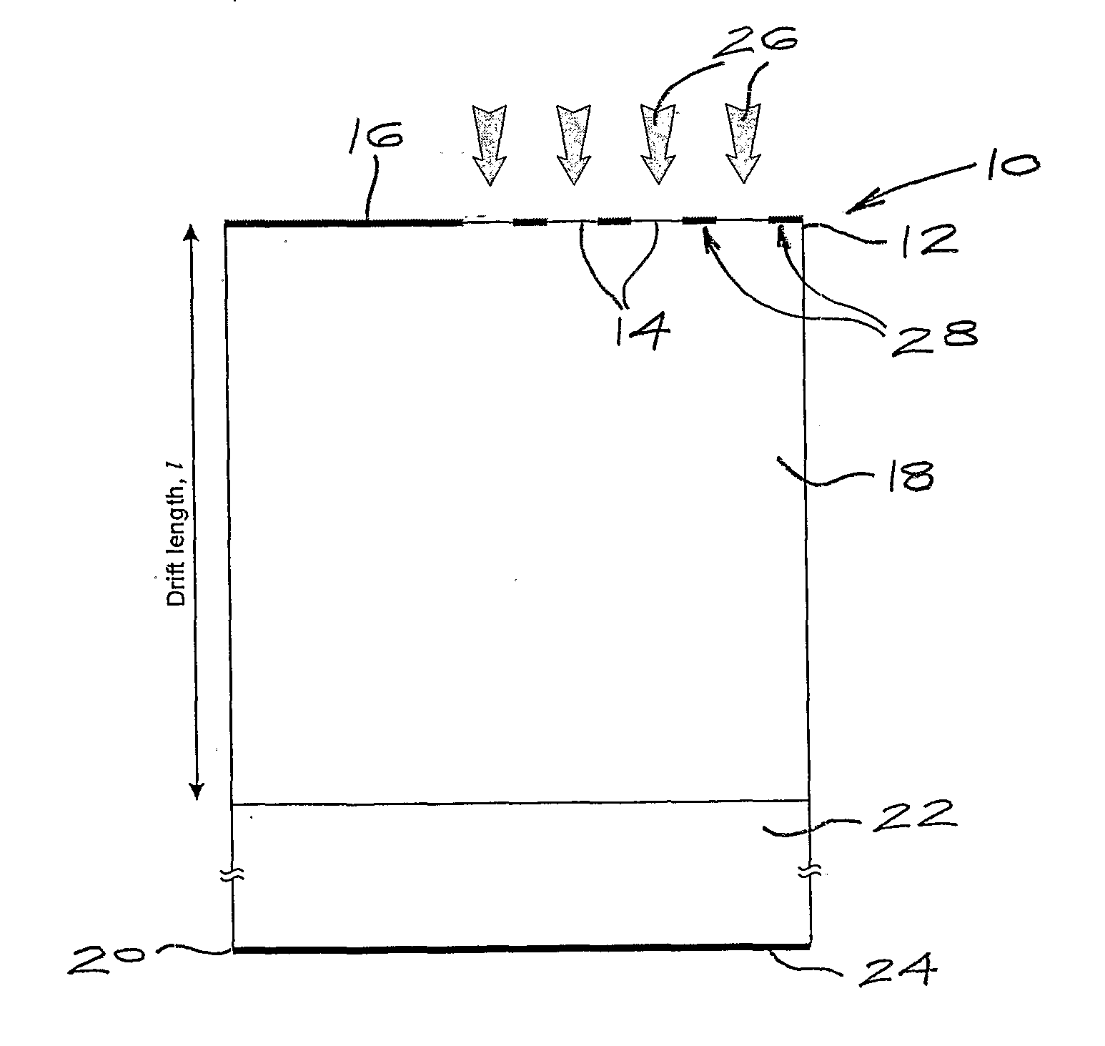
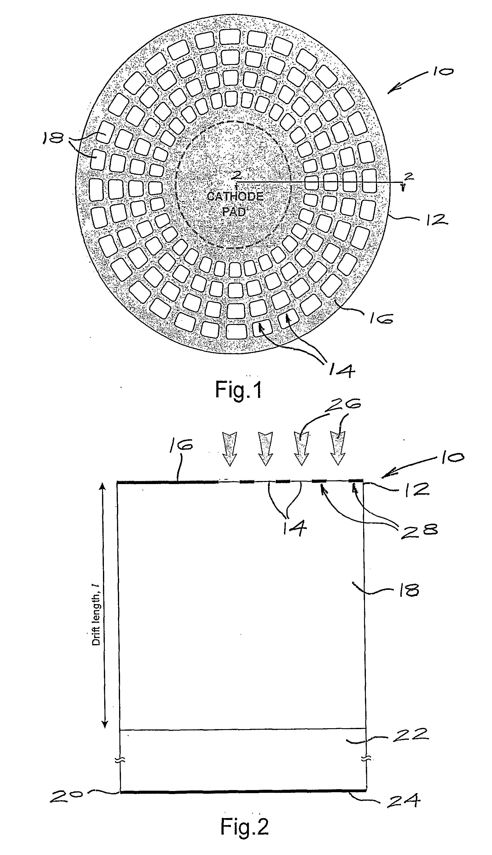
[0056]The device of the invention has been modelled using ISE-TCAD simulations, and using the following conditions:

[0057]Optical excitation by 0.225 μm light, using an absorption coefficient at 300 K of 12 cm−1, and beam intensities of 0.88×10⁻³ W / cm2 to 0.88×10² W / cm2. The Schottky cathode contact comprised a gold contact, with a characteristic lateral dimension of 2.5 μm, with 2.5 μm spacing. The Schottky barrier height was 1.87 eV. The intrinsic diamond layer, called the drift layer, onto which this contact bonded was modelled as containing 1×1013 cm−3 activated B atoms since a layer modelled with zero extrinsic carriers was unrealistic, with then a boron doped layer with 1×1019 cm−3 activated B atoms and a metal contact were used to form the ohmic anode contact. The thickness of the drift layer was varied from 0.2 μm-18 μm.

[0058]The majority of the light is absorbed in the first 2 μm of diamond, although the absorption tail extends beyond 5 μm. This is due to the low absorption ...


PUM


Abstract

A high voltage diamond based switching device capable of sustaining high currents in the on state with a relatively low impedance and a relatively low optical switching flux, and capable of being switched off in the presence of the high voltage being switched. The device includes a diamond body having a Schottky barrier contact, held in reverse bias by the applied voltage to be switched, to an essentially intrinsic diamond layer or portion in the diamond body, a second metal contact, and an optical source or other illuminating or irradiating device such that when the depletion region formed by the Schottky contact to the intrinsic diamond layer is exposed to its radiation charge carriers are generated. Cain in the total number of charge carriers then occurs as a result of these charge carriers accelerating under the field within the intrinsic diamond layer and generating further carriers by assisted avalanche breakdown.

Description

BACKGROUND OF THE INVENTION[0001]This invention relates to a switching device, and in particular to a photoconductive or other irradiation activated switching device fabricated from diamond.[0002]The ideal high voltage switch provides a perfect current block in the ‘off’ state, able to withstand the high voltages applied without breakdown, and in the ‘on’ state has zero impedance to the current being switched, even where this current is high. All practical switching materials and devices fall short of this ideal, and an area of particular difficulty is in switches required to withstand both high voltages in the ‘off’ state and high currents in the ‘on’ state.[0003]As the voltage rating of a system incorporating a high voltage switch increases, the switch used needs to withstand higher voltages in the off state, such that the reverse blocking capability of the switch needs to be as high as possible. Using silicon for such a switch would involve excessively large voltage blocking laye...

Claims


Application Information

Patent Timeline
IPC IPC(8): H01L31/10H01J47/00
CPCH01L31/028H01L31/0288Y02E10/547H01L31/118H01L31/108
Inventor AMARATUNGA, GEHAN ANIL JOSEPHBREZEAU, MIHAIRASHID, JEREMY SUHAILRUPESINGHE, NALIN LALITHTAJANI, ANTONELLA
Owner ELEMENT SIX LTD
Why Eureka
Try Eureka