

Semiconductor memory device
a memory device and semiconductor technology, applied in the field of semiconductor memory devices, can solve the problems of increasing transistor size and not considering the rise speed of the word line, and achieve the effects of reducing the drivability of the access transistor in the memory cell, and improving the snm at the time of reading
- Summary
- Abstract
- Description
- Claims
- Application Information
AI Technical Summary
Benefits of technology
Problems solved by technology
Method used
Image

Examples
first embodiment
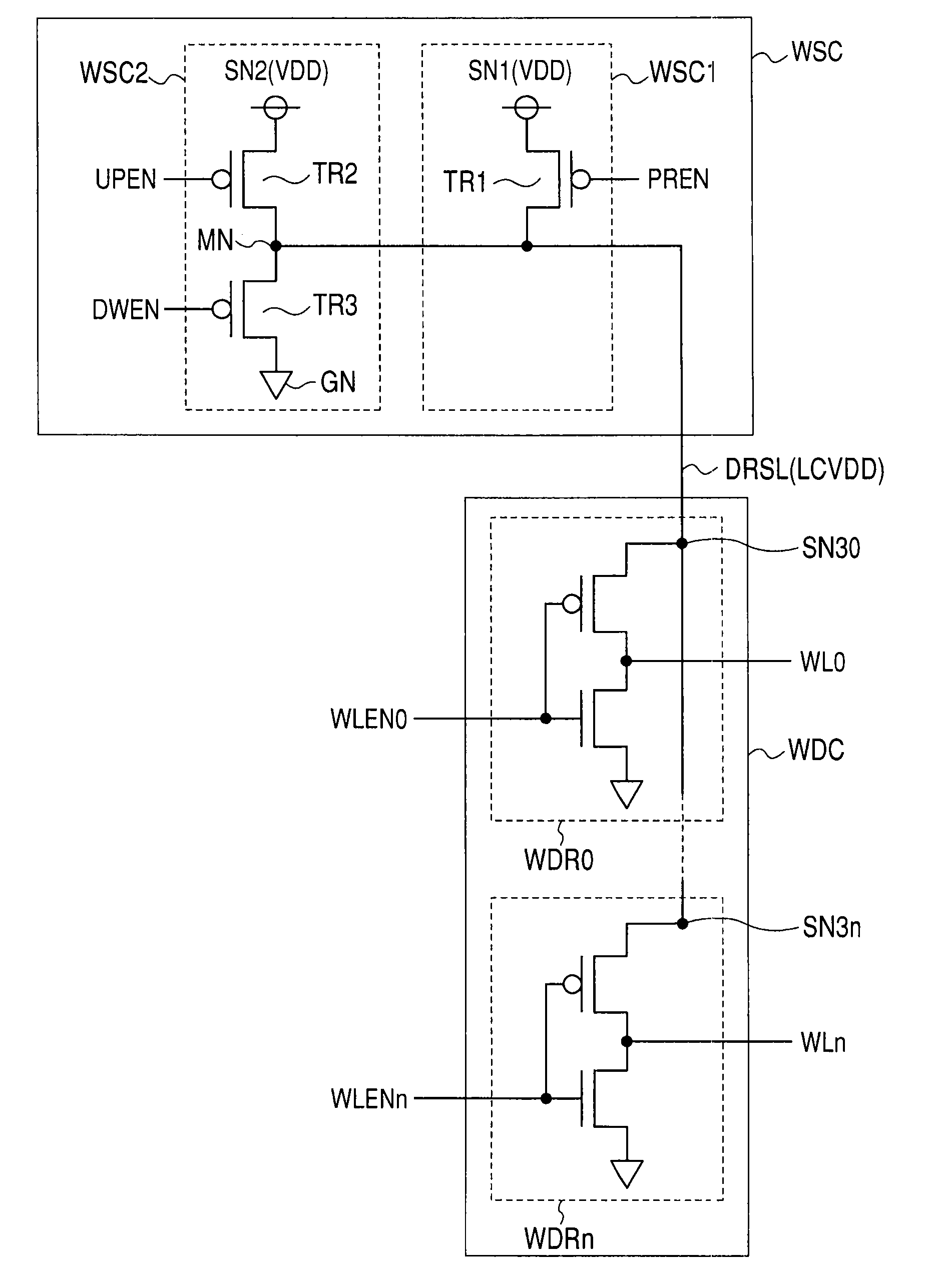
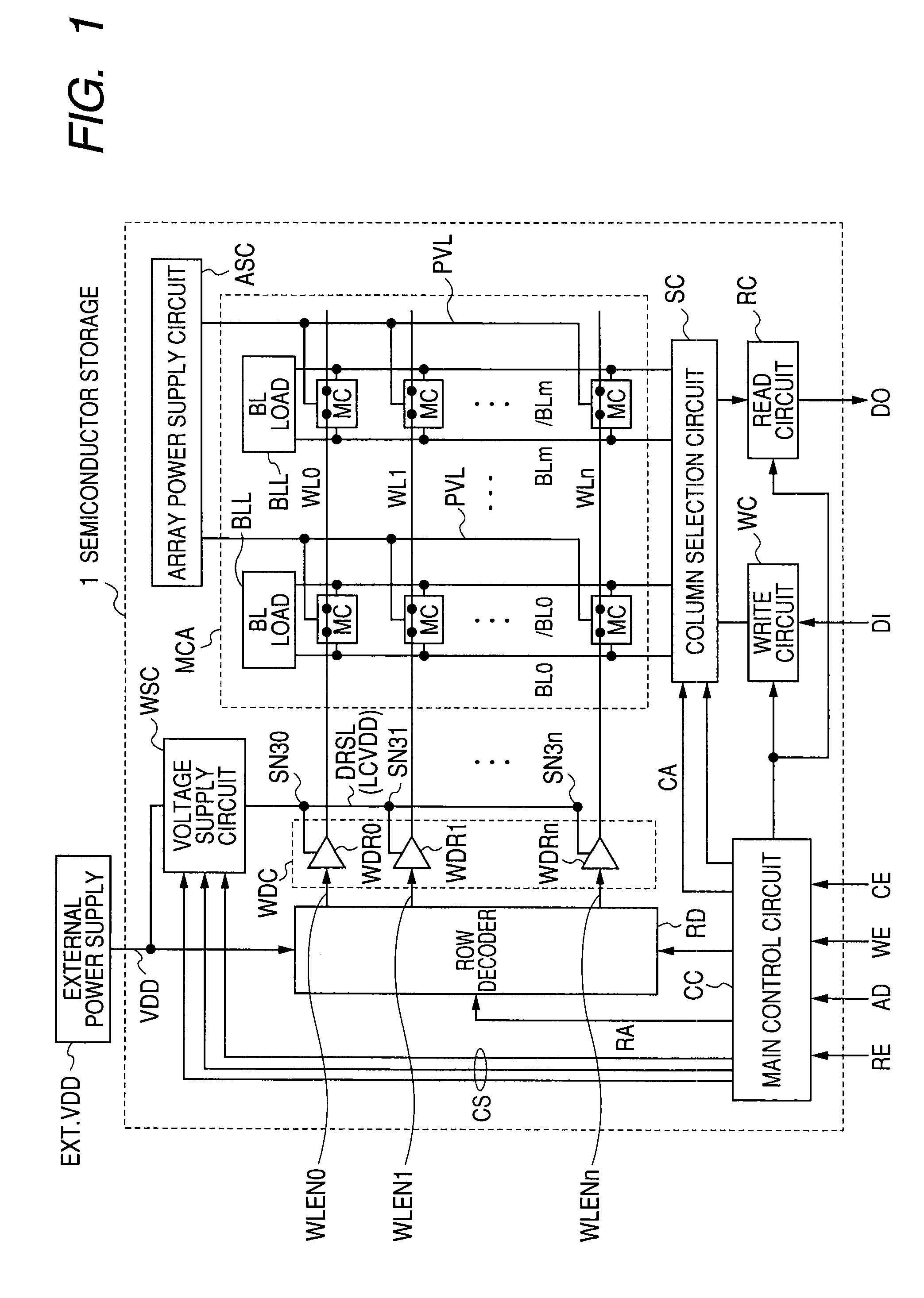
[0033]FIG. 1 is a diagram schematically showing a general configuration of a semiconductor memory device 1 as a first embodiment. In FIG. 1, the semiconductor memory device 1 includes a memory cell array MCA in which memory cells MC are arranged in a matrix. In FIG. 1, as an example, the memory cells MC are arranged in “n” rows and “m” columns in the memory cell array MCA.
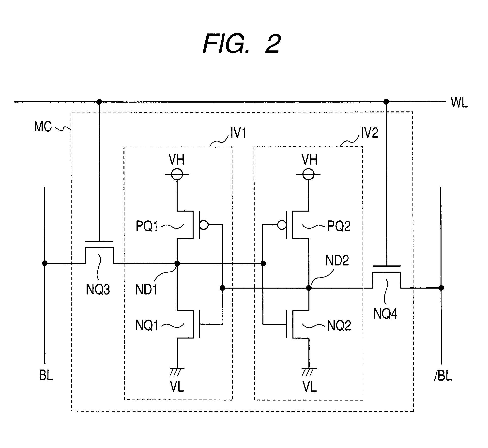
[0034]Word lines WL0 to WLn are arranged in correspondence with the rows of the memory cells MC, and the memory cells MC are connected to word lines WL of the corresponding rows. Bit line pairs BL0 and / BL0 to BLm and / BLm are disposed in correspondence with the columns of the memory cells MC. The memory cell MC is a static memory cell and complementary data is transmitted to the complementary bit line pairs BL0 and / BL0 to BLm and / BLm.
[0035]In correspondence with each of the pairs of bit lines BL and / BL, a bit line load (BL load) BLL is provided. At the time of reading memory cell data, the bit line load BLL pul...
second embodiment
[0097]FIG. 10 is a diagram schematically showing a voltage supply circuit WSC and its periphery as a second embodiment of the invention. The configuration of the voltage supply circuit WSC shown in FIG. 10 is different from that of the voltage supply circuit WSC shown in FIG. 3 with respect to the point that a MOS capacitor MCAP is disposed in the source line DRSL of the word line driver (driver power supply line). The other configuration of the circuit shown in FIG. 10 is the same as that of FIG. 3. The same reference numerals are designated to corresponding parts and their detailed description will not be repeated.
[0098]In the first embodiment, the wiring capacity of the source line DRSL of the word line driver (driver power supply line) is used. By using a voltage accumulated in the wiring capacity, the speed of rising of the word line WL is increased. That is, when the wiring capacity of the source line DRSL of the word line driver (driver power supply line) is large, the speed ...
third embodiment
[0101]FIG. 11 is a diagram showing a voltage supply circuit WSC and its periphery according to a third embodiment of the invention. The configuration of the voltage supply circuit WSC shown in FIG. 11 is different from that of the voltage supply circuit WSC shown in FIG. 3 with respect to the point that a wire WI extends in the word line WL direction in addition to the normal wire of the word line driver source line DRSL (driver power supply line). The parasitic capacitance of the wire WI is used as capacitance of holding the precharge voltage of the driver power supply line DRSL.
[0102]The other configuration of the circuit shown in FIG. 11 is the same as that of FIG. 3. The same reference numerals are designated to corresponding parts and their detailed description will not be repeated.
[0103]FIG. 12 shows an example of the configuration of a semiconductor chip CH of a system LSI (Large Scale Integration). In FIG. 12, on the semiconductor chip CH, a number of functions such as a log...
PUM
 Abstract
Description
Claims
Application Information