Structure of semiconductor device package and method of the same

a semiconductor device and semiconductor technology, applied in the direction of basic electric elements, electrical apparatus contruction details, association of printed circuit non-printed electric components, etc., can solve the problems of time-consuming manufacturing process, inability to meet the demand of producing smaller chips with high density elements on the chip, and complicated semiconductor devices

a semiconductor device and semiconductor technology, applied in the direction of basic electric elements, electrical apparatus contruction details, association of printed circuit non-printed electric components, etc., can solve the problems of time-consuming manufacturing process, inability to meet the demand of producing smaller chips with high density elements on the chip, and complicated semiconductor devices

US20080217761A1Inactive Publication Date: 2008-09-11ADVANCED CHIP ENG TECH

Image

  • Structure of semiconductor device package and method of the same
  • Structure of semiconductor device package and method of the same
  • Structure of semiconductor device package and method of the same

Examples


Embodiment Construction

[0030]In the following description, numerous specific details are provided in order to give a through understanding of embodiments of the invention. Referring now to the following description wherein the description is for the purpose of illustrating the preferred embodiments of the present invention only, and not for the purpose of limiting the same. One skilled in the relevant art will recognize, however, that the invention may be practiced without one or more of the specific details, or with other methods, components, materials, etc.

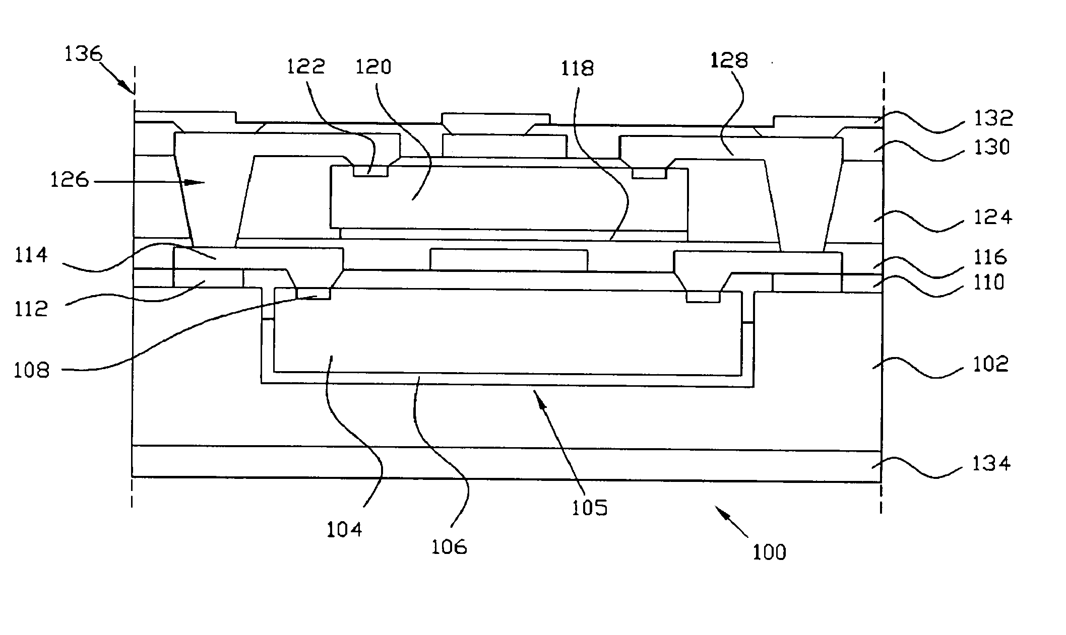
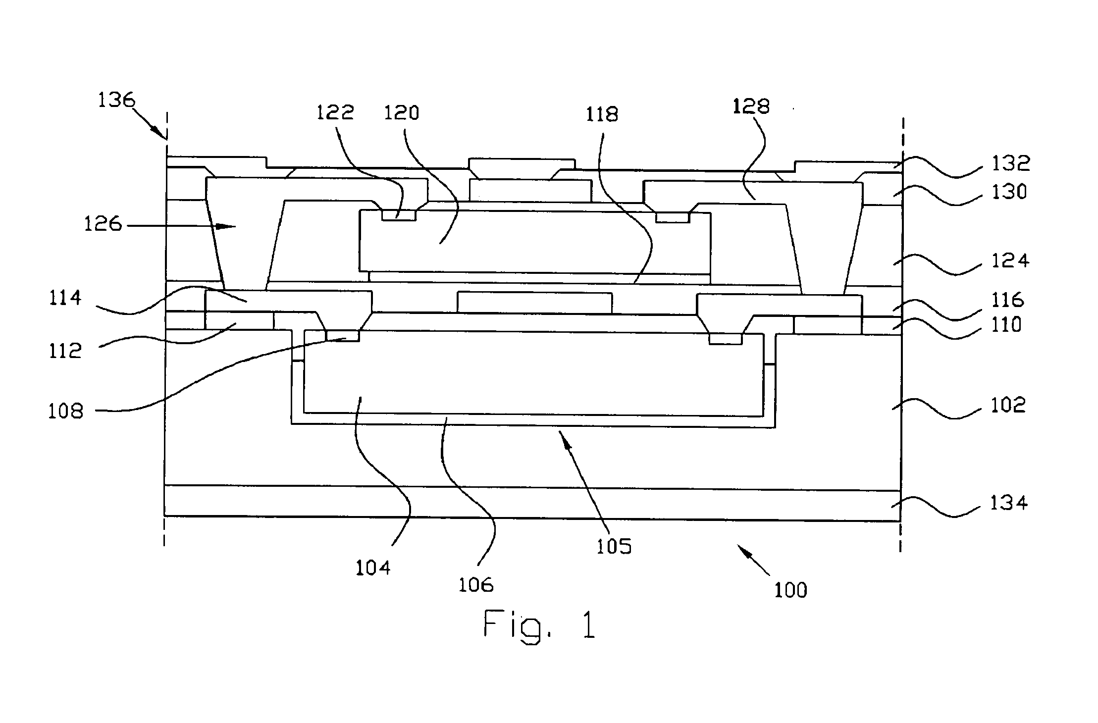
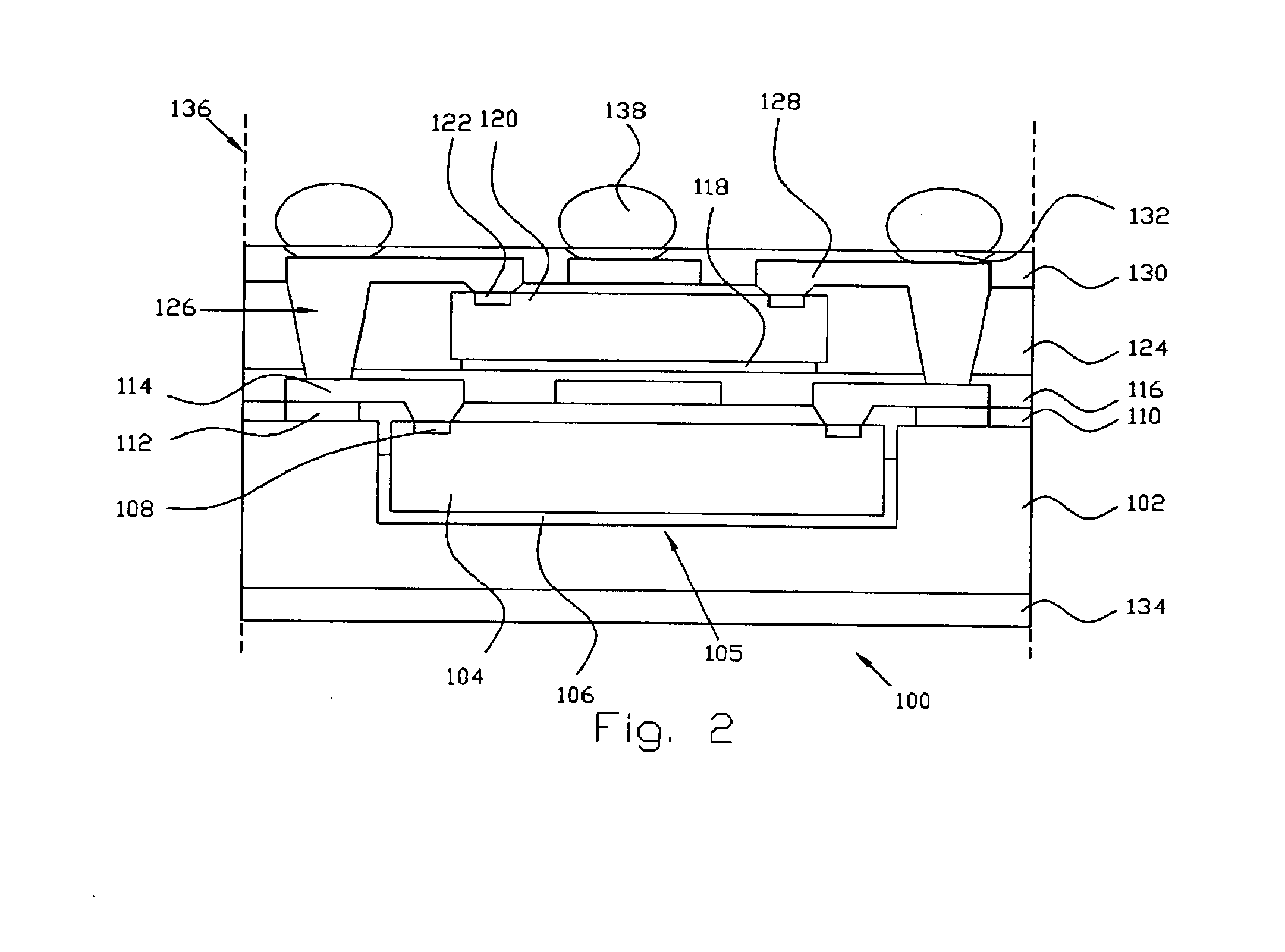
[0031]The present invention discloses a structure of semiconductor device package utilizing a substrate having predetermined terminal contact metal pads formed thereon and a pre-formed cavity formed into the substrate. A die is disposed within the die receiving cavity by adhesion. A photosensitive material is coated over the die and the pre-formed substrate. Preferably, the material of the photosensitive material is formed of elastic material.

[0032]Re...


PUM


Abstract

The present invention provides a semiconductor device package comprising a substrate with at lease a pre-formed die receiving cavity formed and terminal contact metal pads formed within an upper surface of the substrate. At lease a first die is disposed within the die receiving cavity. A first dielectric layer is formed on the first die and the substrate and refilled into a gap between the first die and the substrate to absorb thermal mechanical stress there between. A first re-distribution layer (RDL) is formed on the first dielectric layer and coupled to the first die. A second dielectric layer is formed on the first RDL, and then a second die is disposed on the second dielectric layer and surrounded by core pastes having through holes thereon. A second re-distribution layer (RDL) is formed on the core pastes to fill the through holes, and then a third dielectric layer formed on the second RDL.

Description

BACKGROUND OF THE INVENTION[0001]1. Field of the Invention[0002]This invention relates to a semiconductor device package, and more particularly to a structure of semiconductor device multi chips package with good CTE matching and method of the same, the multi chips package structure can simplify the process to avoid die shift and warp issue during process.[0003]2. Description of the Prior Art[0004]In recent years, the high-technology electronics manufacturing industries launch more feature-packed and humanized electronic products. Rapid development of semiconductor technology has led to rapid progress of a reduction in size of semiconductor packages, the adoption of multi-pin, the adoption of fine pitch, the minimization of electronic components and the like. The purposes and the advantages of wafer level package includes decreasing the production cost, decreasing the effect caused by the parasitic capacitance and parasitic inductance by using the shorter conductive line path, acqui...

Claims


Application Information

Patent Timeline
11 Sep 2008
Publication
US20080217761A1
IPC
H01L23/053
CPC
H01L23/5389; H01L2224/12105; H01L24/82; H01L24/97; H01L25/0652; H01L25/0655; H01L25/0657; H01L25/50
Inventors
YANG, WEN-KUN; CHEN, CHIH-MING