Injector Emitter

a technology of emitter and emitter, which is applied in the field of optoelectronic technology, can solve the problems of limited efficiency increase, and achieve the effects of low internal optical loss, high emission extraction efficiency, and increased emitter efficiency

Inactive Publication Date: 2008-09-11
GENERAL NANO OPTICS
View PDF14 Cites 1 Cited by
  • Summary
  • Abstract
  • Description
  • Claims
  • Application Information

AI Technical Summary

Benefits of technology

[0022]The technical result is also achieved through the fact that the Emitter contains corresponding epoxy substance having appropriate form and corresponding value of the refraction index. This corresponding epoxy substance is placed on the emission output side. Through this corresponding angular distribution of the output emission and increase of the Emitter efficiency are achieved.
[0023]Essence of the present invention consists in creation in its integral execution of the new type of the Emitter with surface output of emission out of the active layer in the form of the great number of beams based on the proposed original effective and non-obvious way of the emission output using properties of the outflow emission. The proposed original and non-obvious key component of the Emitter: emission generation region—emission output region, distributed along the whole length (in principle unlimited) of the Emitter secures effective capture (collection) of emission into optical waveguide of the generation region with the following effective outflow out of the output region in the form of outflow emission with controlled directivity and divergence. The Emitter is characterized by in principle not limited dimensions, by high emission extraction efficiency, by low internal optical losses, by low Joule losses, by low density of the emission power on the output facets, and consequently this secures achievement of technical results listed on the page 2.

Problems solved by technology

But further increase of efficiency is limited by the indicated part of the directed spontaneous emission which is determined by the proposed versions of the emitters-prototypes in which capture of the spontaneous emission into the waveguide and its output in the form of the directed output leaky emission are spatially combined.

Method used


Image

  • Injector Emitter
  • Injector Emitter
  • Injector Emitter

Examples


Embodiment Construction

[0040]In the following the invention is explained through the versions of its realization with references to the enclosed drawings. The presented examples of modifications of the Emitter aren't unique and assume presence of other realizations including certain ranges of wave lengths the features of which are reflected in the set of features of the Claims.

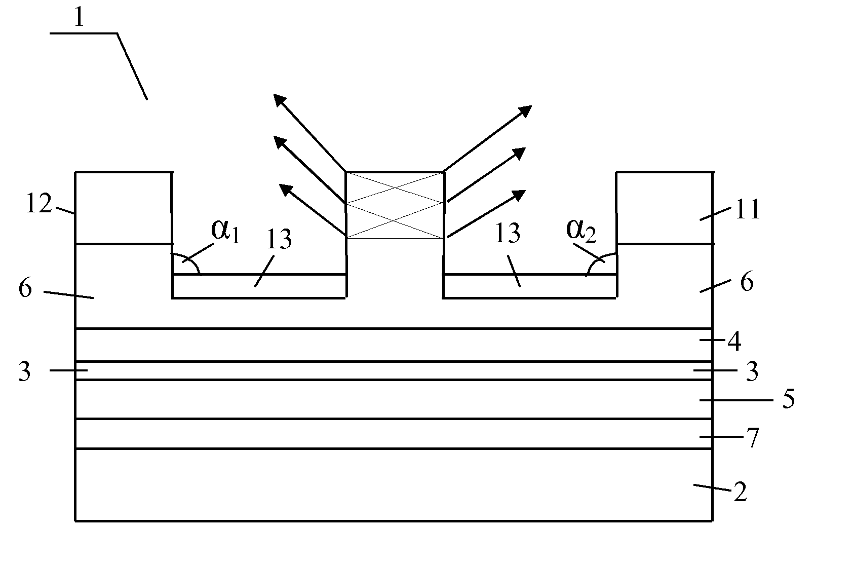
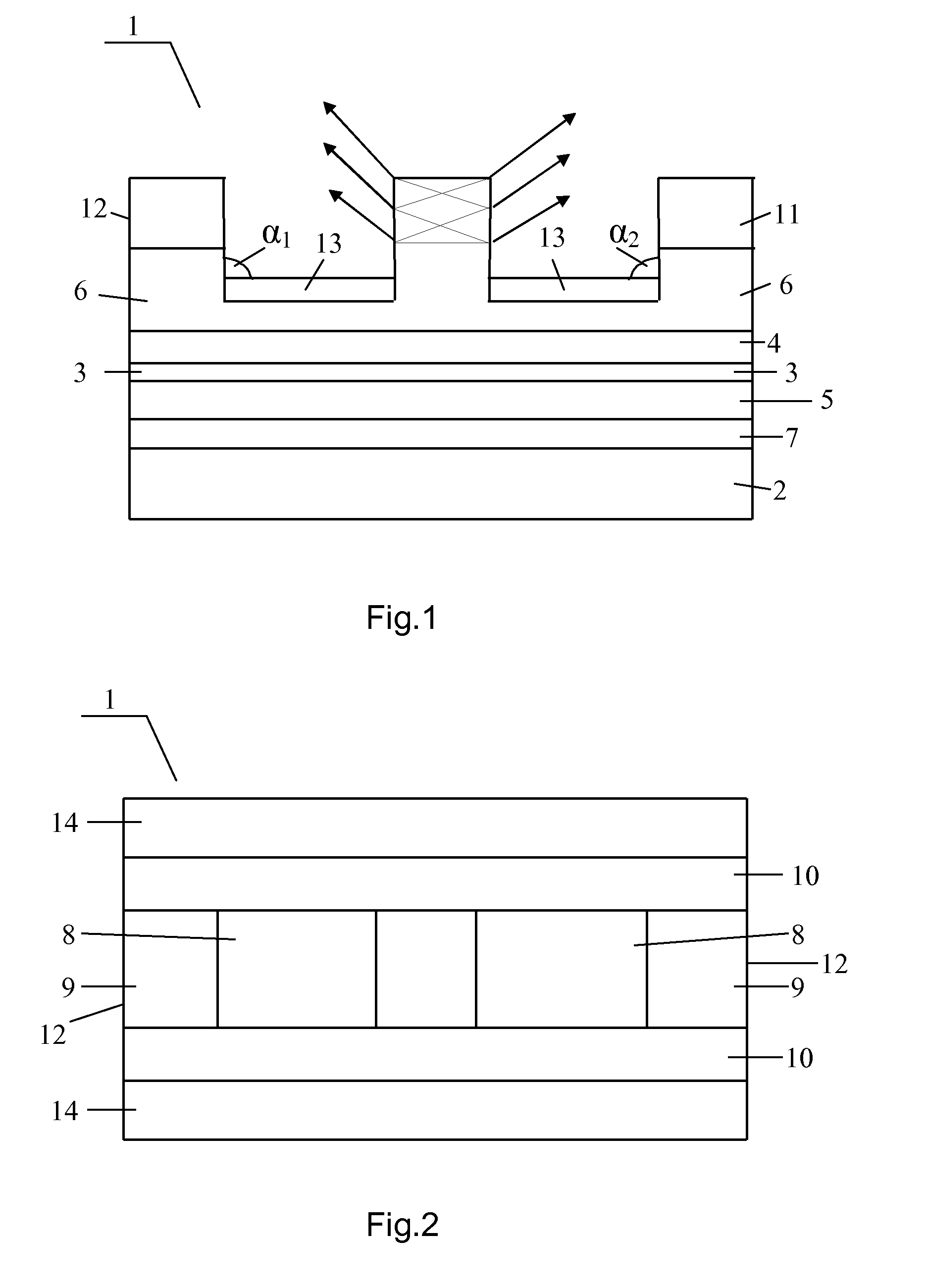
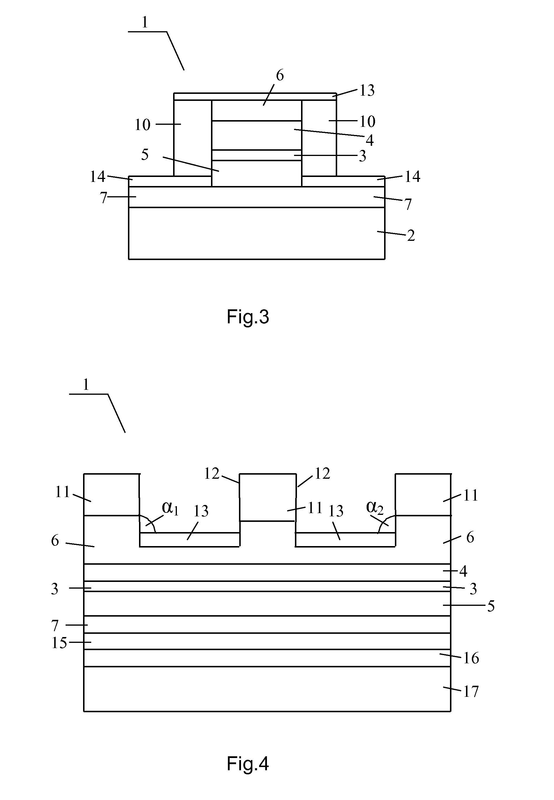
[0041]The proposed Emitter 1 (see FIG. 1-3) contains the heterostructure on the substrate 2 based on the AlGaInN compounds with the active layer 3 of InGaN, the waveguide layers 4, 5, and the confining layers 6, 7 of AlGaN, correspondingly, on the side of the emission output and on the side opposite to it, namely—on the side of the substrate 2. Non-conducting sapphire (Al2O3) having the refraction index of 1.77 is used as the substrate 2. The wavelength of the laser emission is chosen equal to 0.45 μm. The sequence of the alternating stripe generation regions 8 and output regions 9 of the Emitter 1 is located in the direction of the...


PUM


Abstract

Injection emitters (light-emitting diodes, superluminescent emitters) are used in the form of highly-efficient solid state radiation sources within a large wavelength range and for wide field of application, including general illumination using white light emitters provided with light-emitting diodes. Said invention also relates to superpower highly-efficient and reliable injection surface-emitting lasers, which generate radiation in the form of a plurality of output beams and which are characterized by a novel original and efficient method for emitting the radiation through the external surfaces thereof.

Description

FIELD OF THE INVENTION[0001]The invention relates to the optoelectronic technology and namely to the effective powerful and compact semi-conducting injection emitters including the light diodes.DESCRIPTION OF THE RELATED ART[0002]Various types of injection emitters are known: the light diodes—[S. Nakamura et al, Appl. Phys. Lett. v. 76, 22, 2000], [S. Nakamura et al, IEEE Journ. Select. Topics Quantum Electron. v. 7, 188, 2001], [Y. Narukawa, Optics & Photonics News, April 2004, pp. 25-29], the superluminiscent emitters—[Gerard A. Alfonse et al. JEEE Journal of Quantum Electronics, vol. 24, No. 12, December 1988, pp. 2454-2457], [A. T. Semenov et al., Electronics Letters, 1993, vol. 29, No. 10, pp. 854-857].[0003]From the standpoint of technical substance and technical problem to be solved the closest injection non-coherent emitter-prototype was described in the following work [V. I. Shveykin, USA, U.S. Pat. No. 6,429,462 B1, Aug. 6, 2004] including the heterostructure, containing t...

Claims


Application Information

Patent Timeline
Patent Type & Authority Applications(United States)
IPC IPC(8): H01S5/042H01L33/20H01L33/08H01S5/323
CPCH01L33/08H01L33/20H01S5/1032H01S5/42H01S5/18H01S5/223H01S5/32341H01S5/1039H01S5/32
Inventor SHVEYKIN, VASILY IVANOVICH
Owner GENERAL NANO OPTICS
Why Eureka
Try Eureka