Semiconductor device and method for manufacturing thereof

a semiconductor chip and semiconductor technology, applied in semiconductor devices, semiconductor/solid-state device details, electrical apparatus, etc., can solve the problems of difficult to reduce the thickness of the second semiconductor chip used in the coc, difficult to satisfy the requirement to reduce the thickness of the second semiconductor chip to less than 100 m, etc., to reduce suppress the damage applied, and reduce the effect of the thickness of the semiconductor devi

Active Publication Date: 2008-09-25
CYPRESS SEMICON CORP
View PDF10 Cites 42 Cited by
  • Summary
  • Abstract
  • Description
  • Claims
  • Application Information

AI Technical Summary

Benefits of technology

[0008]In view of the aforementioned difficulties, it is an object of the invention to ensure reduction of the semiconductor device thickness, and to suppress the damage applied to the first semiconductor chip.
[0009]According to an aspect of the present invention, there is provided a semiconductor device including a first semiconductor chip, a second semiconductor chip flip-chip bonded to the first semiconductor chip, a resin portion for sealing the first semiconductor chip and the second semiconductor chip such that a lower surface of the first semiconductor chip and an upper surface of the second semiconductor chip are exposed and a side surface of the first semiconductor chip is covered, and a post electrode which pierces the resin portion and is connected to the first semiconductor chip. In the aforementioned structure, the side surface of the first semiconductor chip is covered with the resin portion to suppress the damage applied to the first semiconductor chip. This also makes it possible to reduce the semiconductor device thickness.
[0010]According to another aspect of the present invention, there is provided a manufacturing method of a semiconductor device including the steps of forming a post electrode on a semiconductor wafer, flip-chip bonding a second semiconductor chip onto the semiconductor wafer, forming a groove in an upper surface of the semiconductor wafer, forming a resin portion on the semiconductor wafer for sealing to cover the post electrode and the second semiconductor chip, performing one of grinding and polishing of the resin portion and the second semiconductor chip such that an upper surface of the post electrode and an upper surface of the second semiconductor chip are exposed, performing one of grinding and polishing of a lower surface of the semiconductor wafer such that the semiconductor wafer is thinner than a depth of the groove, so as to form a first semiconductor chip from the semiconductor wafer, and cutting the resin portion along the groove to separate the first semiconductor chip. In the method according to the invention, grinding or polishing is performed in the state where the resin portion and the second semiconductor chip are flip-chip bonded onto the semiconductor wafer so as to reduce the thickness of the second semiconductor chip. As the second semiconductor chip is protected by the resin portion, the second semiconductor chip may be prevented from being cracked. The semiconductor wafer is subjected to the grinding or polishing to reduce its thickness to be smaller than the depth of the groove. The resin portion is cut along the groove to separate the first semiconductor chip. This makes it possible to cover the side surface of the first semiconductor chip with the resin portion.

Problems solved by technology

In the case where the second semiconductor chip is flip-chip bonded onto the first semiconductor chip for increasing the packaging density, it is difficult to satisfy the requirement to reduce the thickness of the second semiconductor chip to less than 100 μm due to difficulty in handling of the thin semiconductor chip from the wafer and the chip tray.
In the case where the flip chip bonding (FCB) is performed with the Au (gold)-Au pressure bonding process, the following difficulty occurs in addition to the difficulty in handling of the semiconductor chip.
Accordingly, it is difficult to reduce the thickness of the semiconductor chip used in the CoC technique for packaging the semiconductor chip through the FCB.
In the process disclosed in Japanese Unexamined Patent Application Publication No. 2000-156461 and Japanese Unexamined Patent Application Publication No. 2004-146728, the side surface of the first semiconductor chip is exposed, which may be damaged during the test or packaging to the interposer.

Method used


Image

  • Semiconductor device and method for manufacturing thereof
  • Semiconductor device and method for manufacturing thereof
  • Semiconductor device and method for manufacturing thereof

Examples


first embodiment

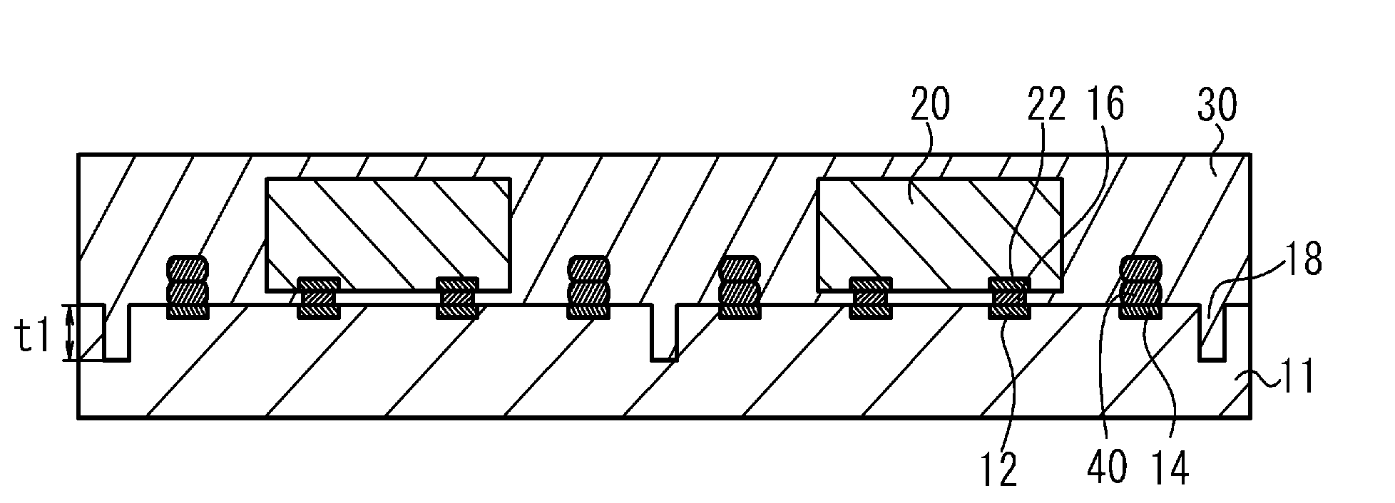
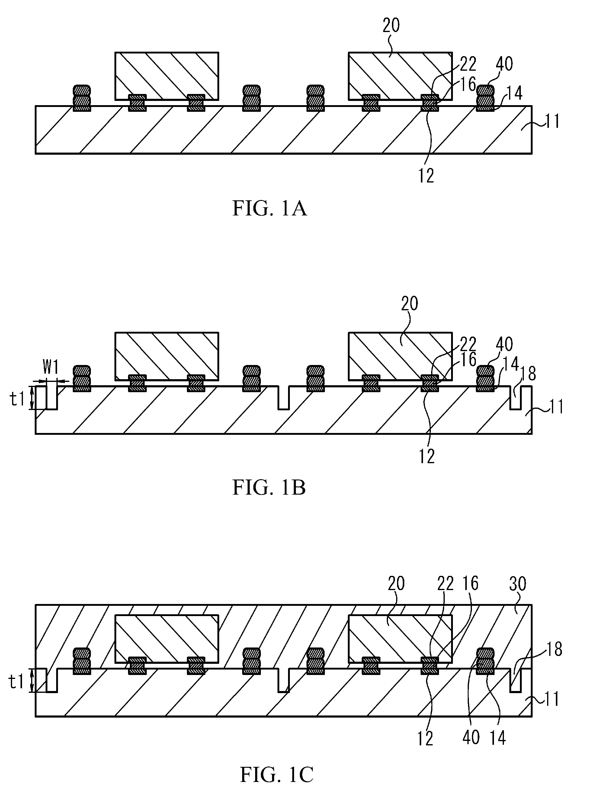
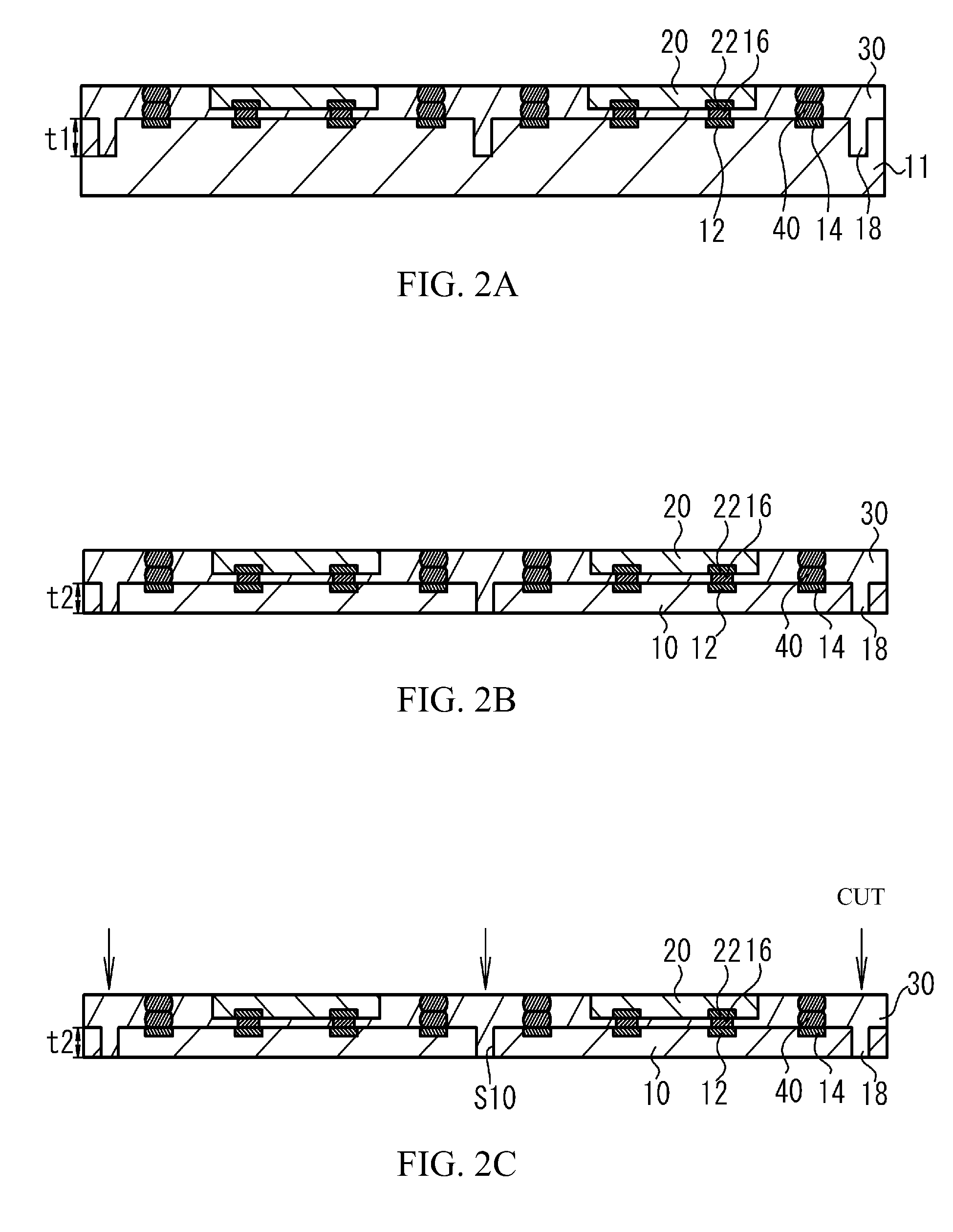
[0027]The method for manufacturing a semiconductor device according to a first embodiment will be described referring to FIGS. 1A to 2C. Referring to FIG. 1A, a post electrode 40 formed of, for example, an Au stud bump is formed on a pad 14 on the upper surface of a silicon semiconductor wafer 11 having a circuit formed on its upper surface. A bump 16 formed of Au, Cu (copper) or solder is formed below a pad 22 on the lower surface of a second semiconductor chip 20 formed of silicon and having a circuit on its lower surface. An interconnection (not shown) allows the electric coupling between the post electrodes 40, between pads 14, and between the post electrode 40 and the pad 14. The second semiconductor chip 20 is flip-chip bonded onto the semiconductor wafer 11 with the bump 16. The thickness of the thus bonded semiconductor wafer 11 and the second semiconductor chip 20 is approximately 750 μm.

[0028]Referring to FIG. 1B, a groove 18 with its width w1 set to 60 μm and its depth t1...

second embodiment

[0039]A second embodiment is an example for packaging the semiconductor device 100 on the interposer. Referring to FIG. 4, the semiconductor device 100 according to the first embodiment is mounted on an insulated interposer 50 (mount portion) formed of the glass epoxy and the like through a die adhesive material 64 such as an adhesive agent. The upper surface of the post electrode 40 is connected to an electrode 54 of the interposer 50 via a bonding wire 62. The semiconductor device 100 is sealed with a sealing portion 60 formed of a resin material. A solder ball 58 is formed on the lower surface of the interposer 50 via an electrode 52. The electrodes 52 and 54 are connected by a connection portion (not shown) provided on the interposer 50. The solder resist 56 is applied onto the lower surface of the interposer 50 so as not to be in contact with the solder ball 58. The semiconductor device 100 has the same structure as that of the first embodiment shown in FIG. 3, and the explanat...

third embodiment

[0042]A third embodiment is an example for forming the post electrode through plating. Referring to FIGS. 5A to 5C, the method for manufacturing the semiconductor device according to the third embodiment will be described. Referring to FIG. 5A, a Cu layer 42 formed of Cu is formed on a pad 14 on the semiconductor wafer 11 through electrolytic plating. The other structure of the embodiment is the same as that of the first embodiment shown in FIG. 1A, and the explanation thereof, thus will be omitted.

[0043]Referring to FIG. 5B, the same manufacturing steps as those of the first embodiment shown in FIGS. 1B and 1C are performed. The resin portion 30 and the second semiconductor chip 20 are ground until the upper surface of the Cu layer 42 is exposed. Referring to FIG. 5C, a Ni layer 44 formed of Ni (nickel) is formed on the Cu layer 42 through nonelectrolytic plating, thus forming a post electrode 46 formed of the Cu layer 42 and the Ni layer 44. The manufacturing steps of the first em...


PUM


Abstract

A semiconductor device which includes a first semiconductor chip, a second semiconductor chip flip-chip bonded to the first semiconductor chip, a resin portion for sealing the first semiconductor chip and the second semiconductor chip such that a lower surface of the first semiconductor chip and an upper surface of the second semiconductor chip are exposed and a side surface of the first semiconductor chip is covered, and a post electrode which pierces the resin portion and is connected to the first semiconductor chip, and a manufacturing method thereof are provided.

Description

CROSS-REFERENCE TO RELATED APPLICATIONS[0001]The present invention is based on Japanese Patent Application No. 2007-070016 filed on Mar. 19, 2007, the entire disclosure of which is hereby incorporated by reference.TECHNICAL FIELD[0002]The invention relates to a semiconductor device and a method for manufacturing thereof, and more particularly to a semiconductor device formed by flip-chip bonding a second semiconductor chip onto a first semiconductor chip and a method for manufacturing thereof.BACKGROUND OF THE INVENTION[0003]The semiconductor device formed by stacking plural semiconductor chips has been under development for the purpose of reducing the packaging density. The CoC (Chip-on-Chip) technique for flip-chip bonding the semiconductor chip onto the other one has been employed to reduce the packaging density.[0004]Japanese Unexamined Patent Application Publication No. 2000-156461 discloses the following technique as shown in FIGS. 8 to 13. That is, the second semiconductor ch...

Claims


Application Information

Patent Timeline
Patent Type & Authority Applications(United States)
IPC IPC(8): H01L23/538H01L21/56
CPCH01L21/561H01L21/568H01L21/78H01L23/3128H01L23/3135H01L24/94H01L25/03H01L25/50H01L2224/48091H01L2224/48145H01L2224/48227H01L2224/94H01L2225/06506H01L2225/0651H01L2225/06513H01L2225/06517H01L2924/01029H01L2924/01078H01L2924/01079H01L2924/15311H01L2924/18161H01L24/48H01L2924/01005H01L2924/01006H01L2924/01033H01L2224/16145H01L21/50H01L24/97H01L2224/97H01L2224/13025H01L2224/16225H01L2224/73209H01L2224/73259H01L24/19H01L2224/0401H01L2224/04042H01L2224/04105H01L2224/32145H01L2224/32225H01L2224/73265H01L2225/06562H01L2224/12105H01L2224/13024H01L2224/73267H01L2224/81H01L2924/00014H01L2924/00012H01L2924/00H01L24/73H01L2924/181H01L24/96H01L2224/45099H01L2224/45015H01L2924/207H01L2224/03
Inventor MEGURO, KOUICHIONODERA, MASANORI
Owner CYPRESS SEMICON CORP
Why Eureka
Try Eureka