Laser array chip, laser module, manufacturing method for manufacturing laser module, manufacturing method for manufacturing laser light source, laser light source, illumination device, monitor, and projector

Inactive Publication Date: 2008-09-25
SEIKO EPSON CORP
View PDF14 Cites 0 Cited by
  • Summary
  • Abstract
  • Description
  • Claims
  • Application Information

AI Technical Summary

Benefits of technology

[0107]By the projector of the invention, the laser light having high level of output power is emitted from th

Problems solved by technology

However, when after connecting the laser element and the submount via the solder, and when the temperature of the laser element and submount is returned to normal temperature, stresses occur within the laser element due to the difference in thermal expansion coefficients of the two members, and so there is the problem in that the service lifetime of the laser element is shortened.
Furthermore, warping of the laser element and submount occurs, and so there is the problem in that scattering occurs in the position of the beam emitted by the laser.
When a material having a linear expansion coefficient close to the linear expansion coefficient of the laser element is used in the submount, the range of materials which can be used is severely limited.
However, AIN has the problems of high cost, and heat dissipation is degraded, due to the fact that the thermal conductivity is approximately 200 W/mK.
As a result, there is the problem in that heat generated by the semiconductor laser element is not easily dissipated.
Furthermore, indium solder is used when connecting a semiconductor laser element to a submount, but there are the problems in that indium (In) solder is easily oxidized, easily diffuses, and is expensive.
Furthermore, when using the method described in the above Japanese Unexamined Patent Application, First Publication No. 2002-299744, which determines the combination of materials used in the laser element, submount, and heat sink, as well as the thickness of the submount, the respective materials which can be used are limited to a narrow range, and moreover the thickness of the submount is also limited.
Consequently, when packaging a semiconduc

Method used


Image

  • Laser array chip, laser module, manufacturing method for manufacturing laser module, manufacturing method for manufacturing laser light source, laser light source, illumination device, monitor, and projector
  • Laser array chip, laser module, manufacturing method for manufacturing laser module, manufacturing method for manufacturing laser light source, laser light source, illumination device, monitor, and projector
  • Laser array chip, laser module, manufacturing method for manufacturing laser module, manufacturing method for manufacturing laser light source, laser light source, illumination device, monitor, and projector

Examples


first embodiment

[0131]A manufacturing method for manufacturing a laser module of this embodiment is explained.

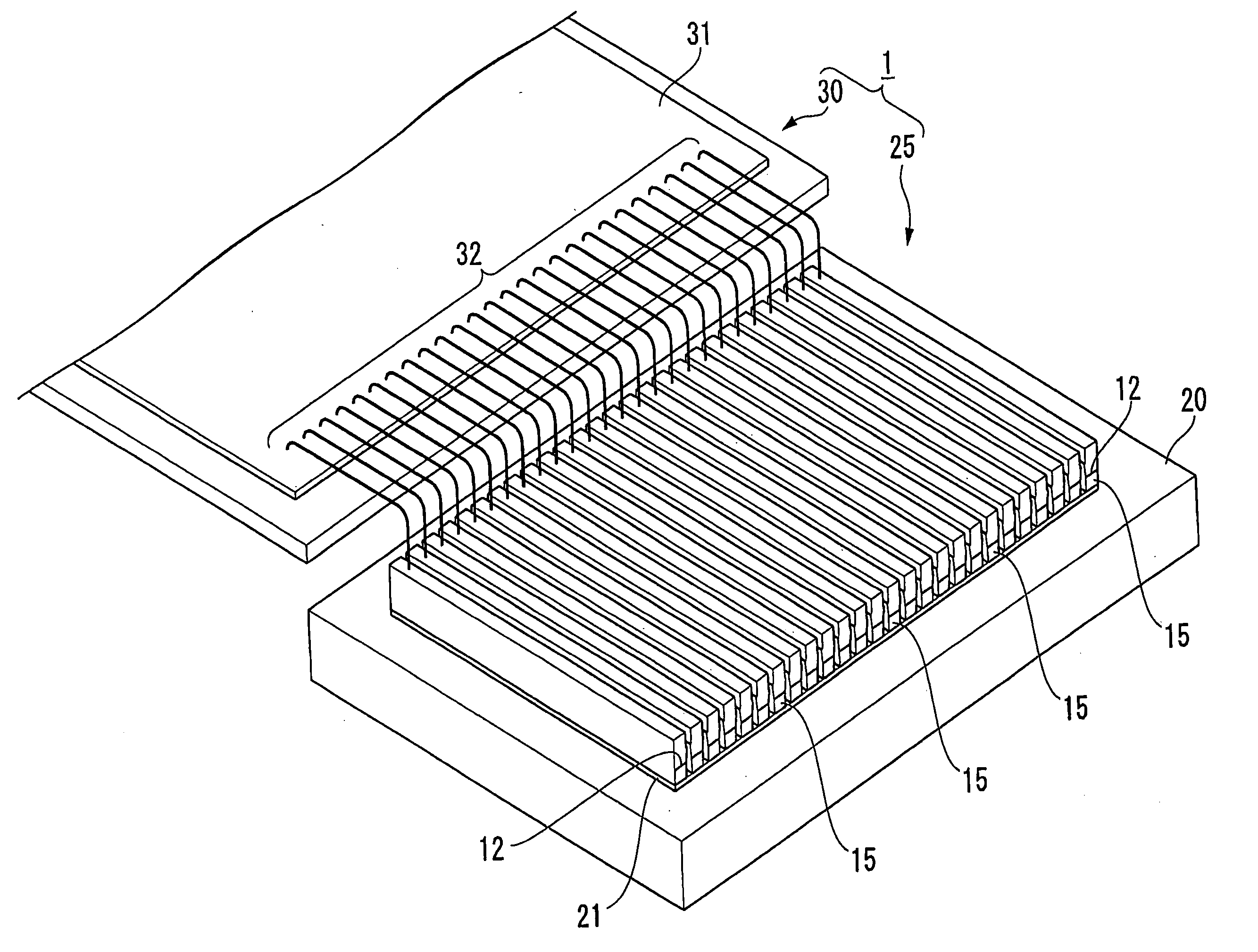
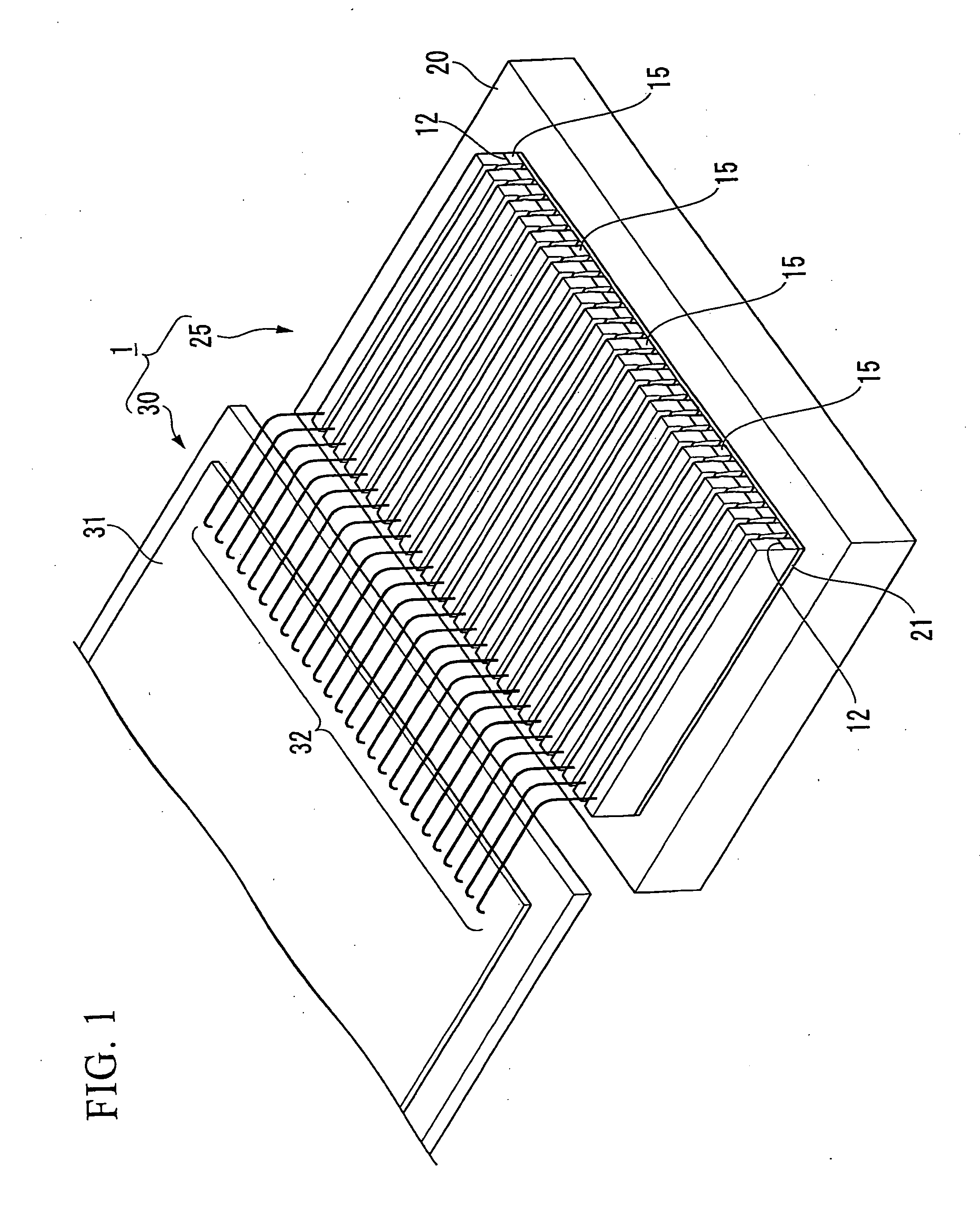
[0132]First, the configuration of the laser module manufactured using the manufacturing method for manufacturing a laser module of this embodiment is explained referring to FIG. 1

[0133]As shown in FIG. 1, the laser module 1 includes a laser light source 25 and a current-supplying substrate 30.

[0134]The laser light source 25 includes a plurality of laser elements 15, a submount 20 (supporting substrate), and a current-supplying substrate 30.

[0135]The submount 20 supports the plurality of laser elements 15, and provides reinforcement to enhance mechanical strength.

[0136]As explained below, the plurality of laser elements 15 are obtained by dividing the laser array chip 10 packaged on the submount 20 into a plurality of laser elements 15.

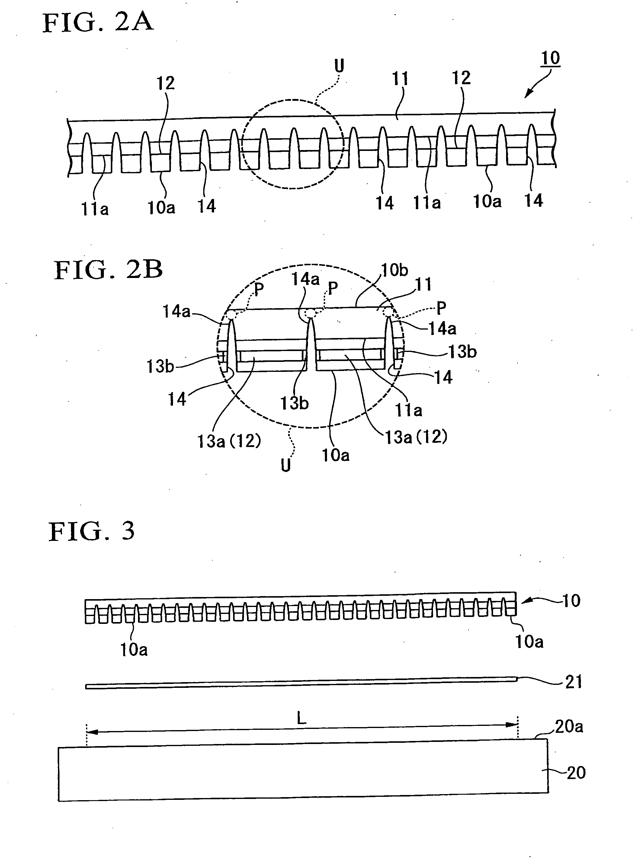
[0137]First, the laser array chip 10 packaged on the submount 20 is explained referring to FIGS. 2A and 2B.

[0138]FIGS. 2A and 2B show a laser array chip of th...

second embodiment

[0207]Next, a second embodiment of the invention is explained, referring to FIG. 10.

[0208]For purposes of simplification, in FIG. 10, a housing of the projector 100 is not shown.

[0209]In the projector 100, a red laser light source device 101R (light source device), a green laser light source device 101G (light source device), and a blue light source device 101B (light source device), which emit red light, green light, and blue light, respectively, are light source devices 101 having laser modules 1 of the above first embodiment.

[0210]The projector 100 includes an image formation device, having liquid crystal light valves 104R, 104G, and 104B (light modulation devices), which modulate the laser light emitted from the laser light source devices 101R, 101G, and 101B, respectively, and a projection lens 107 (projection device), which enlarges and projects images formed by the liquid crystal light valves 104R, 104G, and 104B onto a screen (display screen) 110.

[0211]Furthermore, the proje...

third embodiment

Laser Light Source

[0228]First, the configuration of the laser light source of a third embodiment to which the invention is applied is explained.

[0229]FIG. 11 shows a plane configuration of the laser light source seen from above (Z direction).

[0230]FIG. 12 shows a side configuration of the laser light source seen from a side (X direction).

[0231]FIGS. 13A and 13B show the laser light source. FIG. 13A shows a side configuration of the laser light source seen from a side (Y direction), and FIG. 13B is an enlarged cross-sectional view showing the area indicated by reference numeral R in FIG. 13A.

[0232]As shown in FIGS. 11 to 13B, the laser light source 60 includes a laser array chip 75 having five laser elements 65, and a submount 80. Also, as shown in FIG. 13A, division sections 61 are formed between the laser elements 65.

[0233]The laser elements 65 have a semiconductor substrate 66, a semiconductor multilayer film 70 serving as a emission section and formed on the semiconductor substra...


PUM


Abstract

A laser array chip includes: a plurality of emission sections emitting laser lights; and a weak section formed in a portion in the thickness direction of at least a portion of the areas between the emission sections, whose strength is weaker than the strength of areas in which the emission sections are formed.

Description

CROSS-REFERENCE TO RELATED APPLICATION[0001]This application is based on and claims priority from Japanese Patent Application No. 2007-074115, filed on Mar. 22, 2007, and Japanese Patent Application No. 2007-076111, filed on Mar. 23, 2007, the contents of which are incorporated herein by reference.BACKGROUND[0002]1. Technical Field[0003]The present invention relates to a laser array chip, a laser module, a manufacturing method for manufacturing a laser module, a manufacturing method for manufacturing a laser light source, a laser light source, an illumination device, a monitor, and a projector.[0004]2. Related Art[0005]Conventionally, semiconductor laser elements are GaAs system edge-emission type semiconductor laser elements formed on GaAs substrate.[0006]Such semiconductor laser elements are not limited to a single emission section. In order to realize a laser having high level of output power, there are constitutions in which a laser array, in which a plurality of emission sectio...

Claims


Application Information

Patent Timeline
IPC IPC(8): H01S5/10H01L33/00H01L21/02
CPCH01S5/02272H04N9/3129H01S5/4031H01S5/02276H01S5/0237H01S5/02345
Inventor EGAWA, AKIRATAKAGI, KUNIHIKO
Owner SEIKO EPSON CORP
Why Eureka
Try Eureka