

Embedded transformable nanofilaments in multilayer crystalline space for photovoltaic cells and method of fabrication
a photovoltaic cell and nano-crystalline technology, applied in the field of photovoltaic cells, can solve the problems of high cost relative to other energy production sources, limited efficiency and high cost, and achieve the effects of maximizing light collection, energy conversion and distribution, and increasing pv cell performan
- Summary
- Abstract
- Description
- Claims
- Application Information
AI Technical Summary
Benefits of technology
Problems solved by technology
Method used
Image

Examples
Embodiment Construction
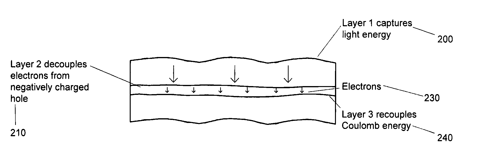
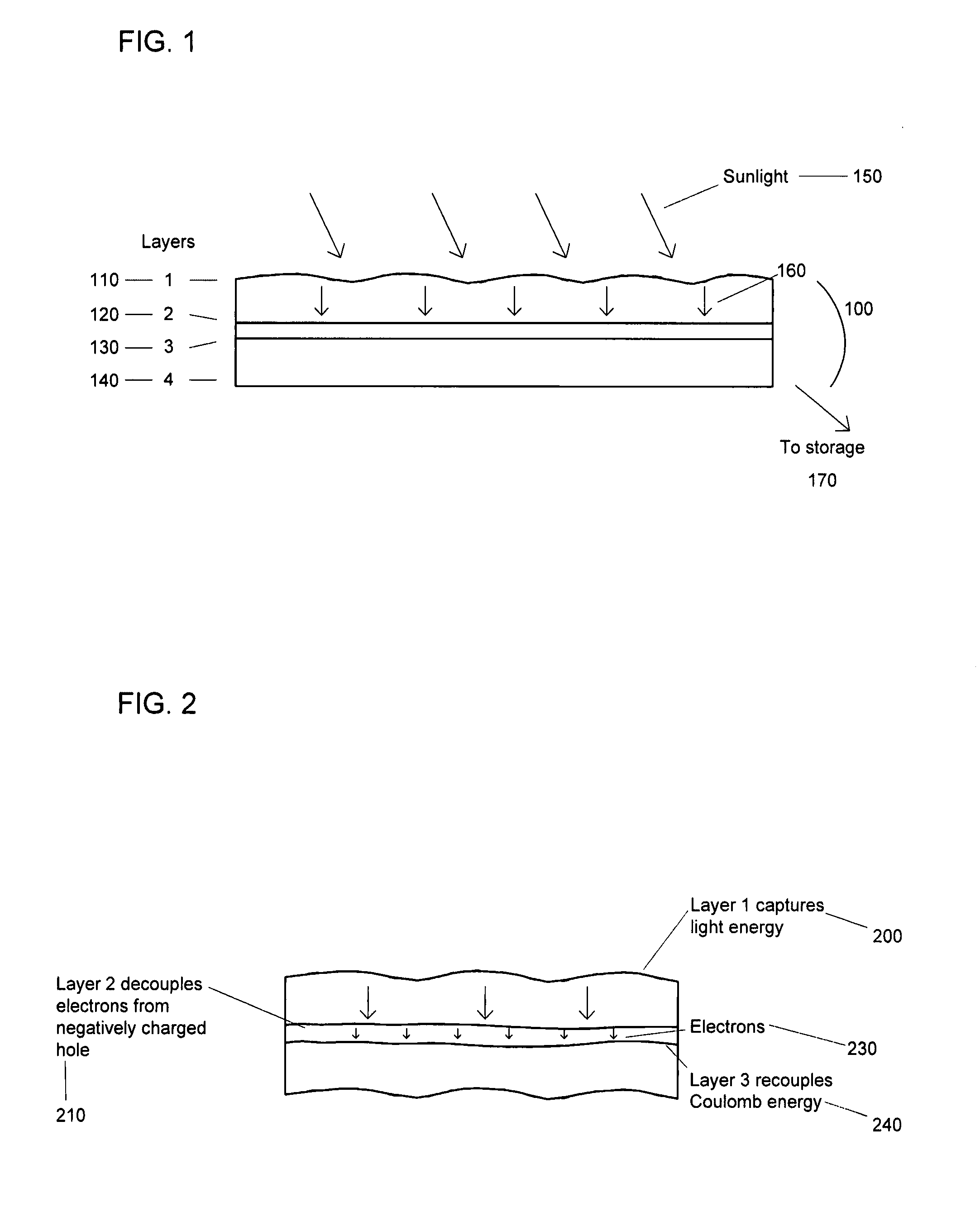
[0018]The present invention has multiple layers, like strata of ultra-thin film that are sandwiched to one another. While the materials vary, these hybrid nanostructures consist of titanium dioxide (for the nanofilaments) and copper indium gallium diselenide (CIGS) or other exotic crystalline materials for the semiconductor stratum.
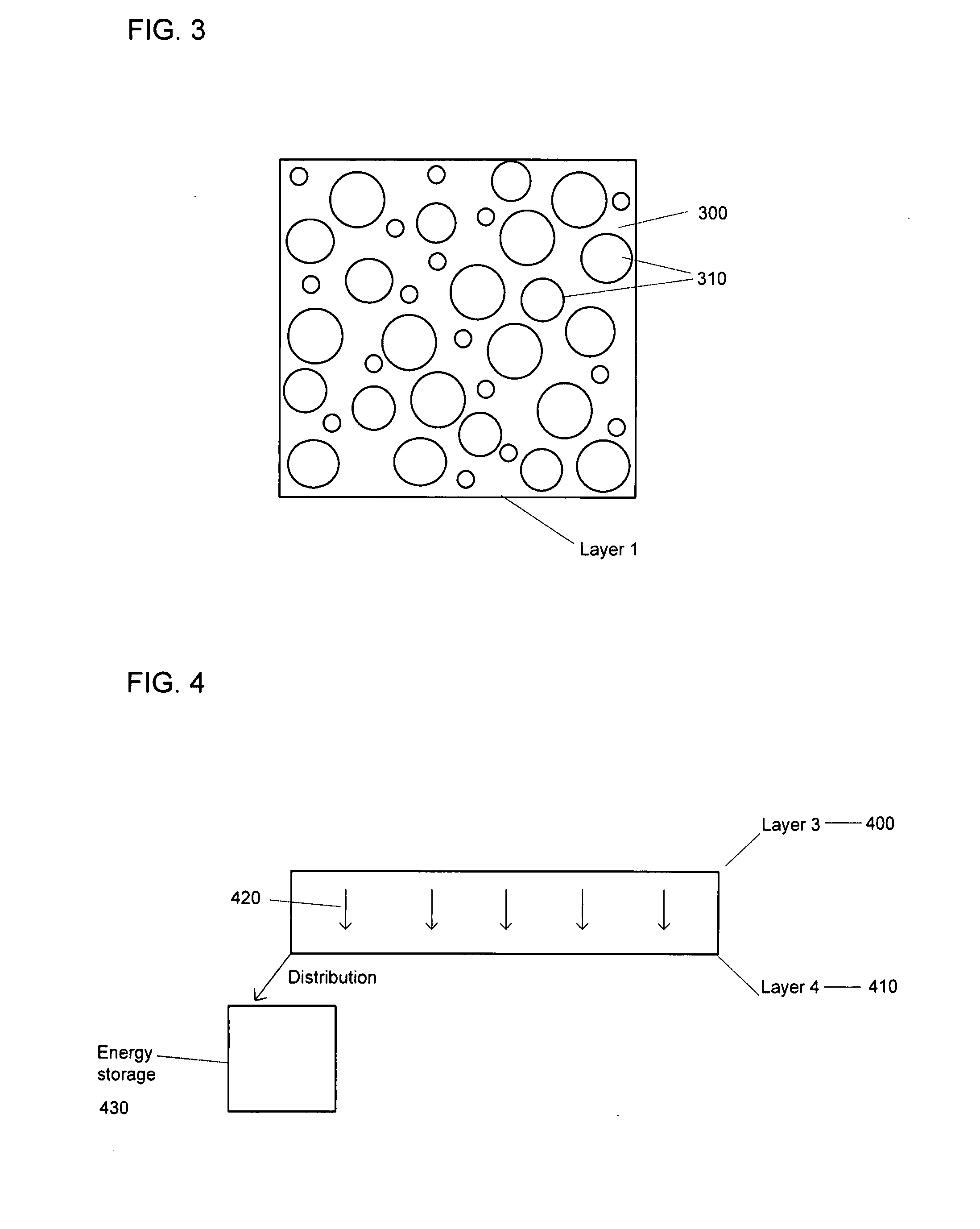
[0019]On the first layer of the PV apparatus, organic circular nanostructures (made of dye) appear in random patterns like raindrops. This layer absorbs the sunlight and transfers the light energy to the second layer. The second and third layers are integrated and consist of charge decoupling and charge recoupling structures. The two connected middle layers link the bottom (fourth) processing layer and the top (first) collection layer. After the second layer decouples electrons from the negatively-charged hole with a nanofilament system, it feeds the electrons to the connected third layer. The third layer recouples the useful Coulomb energy of the electro...
PUM
| Property | Measurement | Unit |
|---|---|---|
| Angle | aaaaa | aaaaa |
| Temperature | aaaaa | aaaaa |
| Energy | aaaaa | aaaaa |
Abstract
Description
Claims
Application Information