

Scanning electron microscope
a scanning electron microscope and electron microscope technology, applied in material analysis using wave/particle radiation, instruments, nuclear engineering, etc., can solve the problems of large primary electron beam, inability to discriminate secondary electrons, and large so as to achieve the effect of conducting the band-pass discrimination of energy without enlarging the primary electron beam aberration
- Summary
- Abstract
- Description
- Claims
- Application Information
AI Technical Summary
Benefits of technology
Problems solved by technology
Method used
Image

Examples
first embodiment
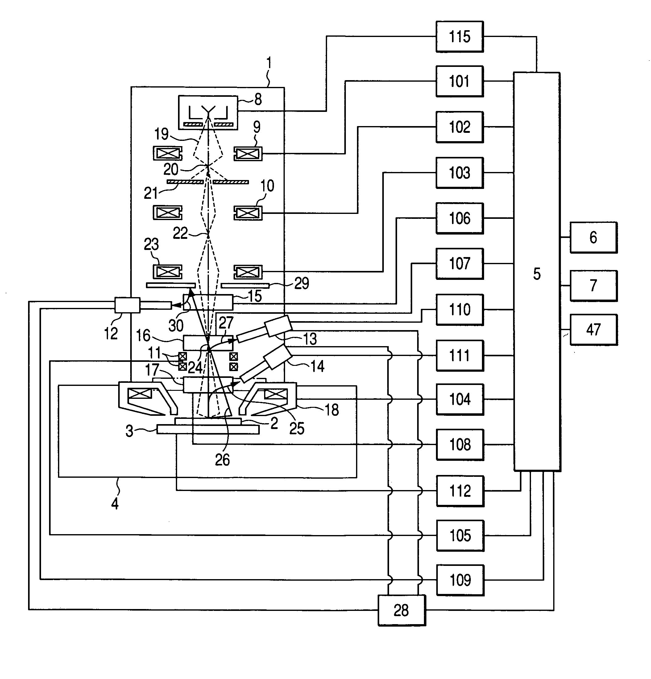
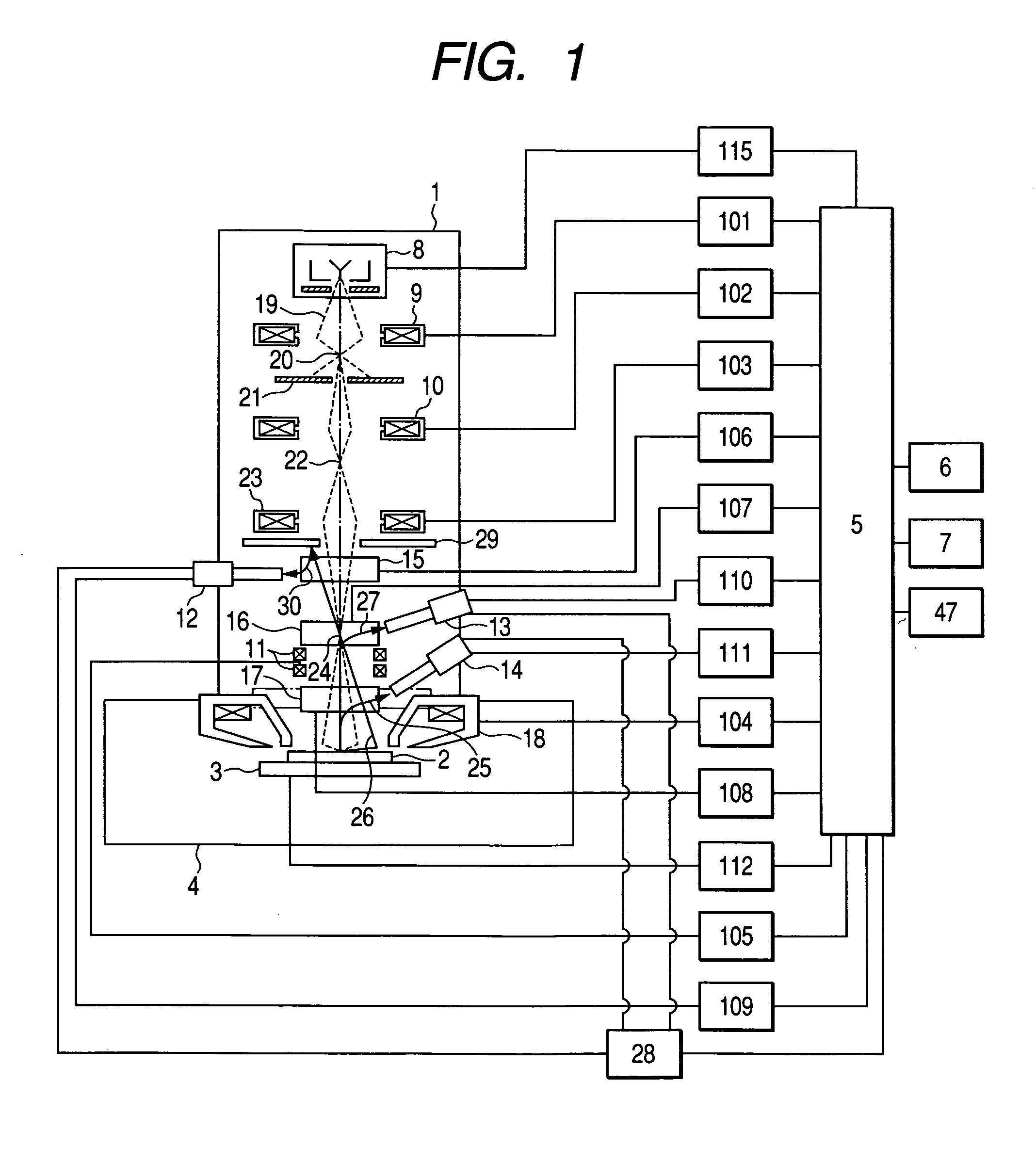
[0037]FIG. 1 shows the entire structural diagram of a scanning electron microscope according to a first embodiment. The scanning electron microscope shown in FIG. 1 is roughly made up of an electron optical body tube 1 having a mechanism for irradiating an electron beam to a specimen, a sample chamber 4 that stores a stage 3 which holds a specimen 2 to be observed, diverse power supplies 101 to 115 for controlling the respective structural parts of the electron optical body tube 1 and the sample chamber 4, an information processing unit that conducts control processing, diverse image processing, or information processing related to a user interface, an image display system 6, and an image memory 7.
[0038]The electron optical body tube 1 includes an electron gun 8, a first condenser lens (C1 lens) 9, a second condenser lens (C2 lens) 10, a third condenser lens (C3 lens) 23, two scanning deflectors 11, a detection unit A12, a detection unit B13, a detection unit C14, a detection unit A...
second embodiment
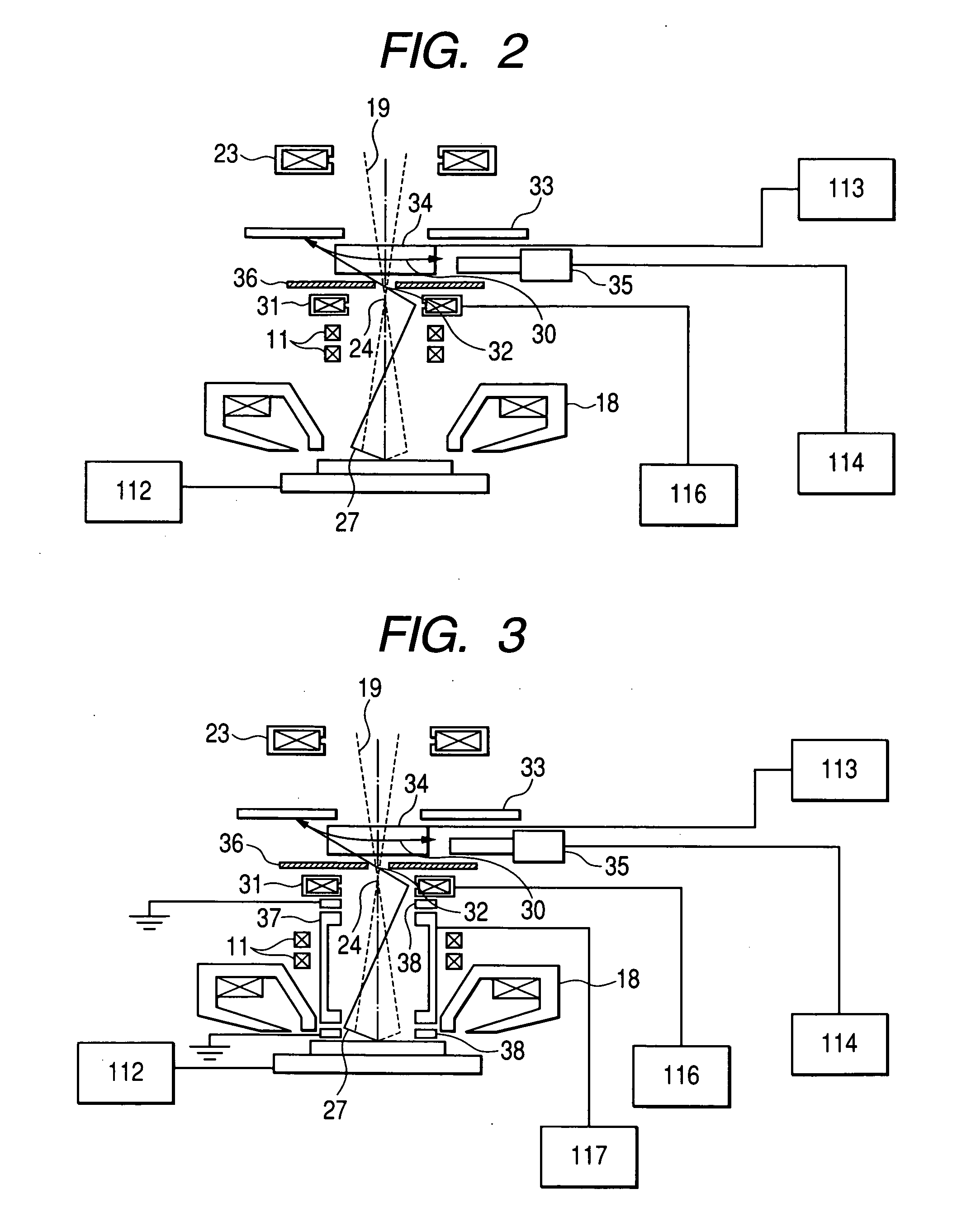
[0076]FIG. 2 shows a part of the structure of a scanning electron microscope according to a second embodiment which is another embodiment of the present invention. The second embodiment is identical with the first embodiment shown in FIG. 1 except for the energy band-pass detection system.
[0077]In the second embodiment, an axisymmetric detection lens 31 that supplies a lens field which converges the secondary particles to the secondary particles is disposed in the third convergent point 24 of the primary electron beam 19 which is formed at a specific position. The lens that functions as the field supply unit is not required to be a magnetic field lens, but can be an electrostatic lens or multiple multi-pole lenses when the same operation is conducted.
[0078]When the energy band-pass detection is conducted, the operator selects a representative value of the energy of the secondary particles 27 to be detected on the interface that is displayed on the image display system 6 as in the fi...
third embodiment
[0090]FIG. 3 shows a third embodiment in which an einzel lens is superimposed on the objective lens 18 of the second embodiment.
[0091]An axisymmetric accelerating electrode 37 is disposed on the electron gun side of the lower surface of the objective lens 18. The boosting voltage that is applied to the accelerating electrode 37 is a high voltage whose absolute value is 1 kV to 10 kV, and is applied by the boosting power supply 117. In order to scan the primary electron beam 18, the scanning deflector 11 of the type that supplies the vibration magnetic field is disposed outside of the accelerating electrode 37. It is necessary that the accelerating electrode 37 is made of nonmagnetic material so as not to shield the vibration magnetic field. Ground electrodes 38 that are axisymmetric and held to the ground potential are disposed above and below the accelerating electrode 37. Alternatively, the upper magnetic path of the objective lens 18 that is the ground potential can be used witho...
PUM
 Abstract
Description
Claims
Application Information