Light emitting diode apparatus

Inactive Publication Date: 2008-10-02
DELTA ELECTRONICS INC
View PDF0 Cites 41 Cited by
  • Summary
  • Abstract
  • Description
  • Claims
  • Application Information

AI Technical Summary

Benefits of technology

[0010]An object of the invention is to provide a light emitting diode apparatus having evenly diffused currents, good thermal conductivity and high opto-electronic conversion efficiency.
[0011]To achieve the above, the invention discloses a light emitting diode apparatus including a heat dissipating substrate, a composite layer, an epitaxial layer, a first electrode and a second electrode. The composite layer includes a reflective layer, a transparent conductive layer and a patterned insulating thermoconductive layer disposed between the reflective layer and the transparent conductive layer. The composite layer is disposed between the heat dissipating substrate and the epitaxial layer and allows currents to concentrate to the reflective layer or the transparent conductive layer and then to be evenly diffused through the transparent conductive layer. The epitaxial layer includes a first semiconductor layer, an active layer and a second semiconductor layer. The first electrode is electrically connected to the first semicond

Problems solved by technology

Thus, the resistance value is too high so that the currents cannot be evenly diffused.
In addition, no path can conduc

Method used


Image

  • Light emitting diode apparatus
  • Light emitting diode apparatus
  • Light emitting diode apparatus

Examples


Embodiment Construction

[0018]The present invention will be apparent from the following detailed description, which proceeds with reference to the accompanying drawings, wherein the same references relate to the same elements.

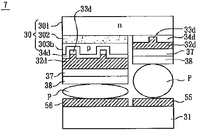
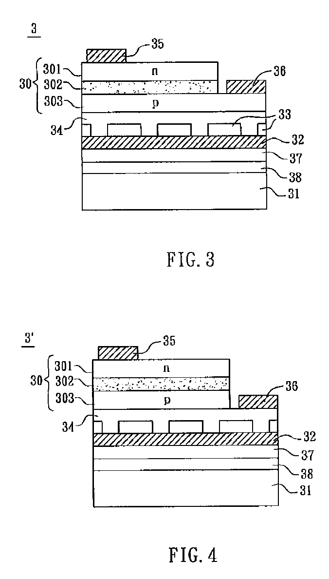
[0019]Referring to FIG. 3, a light emitting diode apparatus 3 according to an embodiment of the invention includes a heat dissipating substrate 31, a composite layer S, an epitaxial layer 30, a first electrode 35 and a second electrode 36.

[0020]The heat dissipating substrate 31 is a permanent substrate having a high coefficient of heat conductivity, and can be made of a metal material, a composite material or an insulating material. In this embodiment, the material of the heat dissipating substrate 31 can be aluminum, copper, aluminum copper oxide, silicon, gallium arsenide, gallium phosphide, silicon carbide, boron nitride, aluminum nitride, a ceramic material or any combination thereof.

[0021]The composite layer S includes a reflective layer 32, a transparent conductive layer 34 and ...


PUM


Abstract

A light emitting diode apparatus includes a heat dissipating substrate, a composite layer, an epitaxial layer, a first electrode and a second electrode. The composite layer includes a reflective layer, a transparent conductive layer and a patterned insulating thermoconductive layer, which is disposed between the reflective layer and the transparent conductive layer. The composite layer is disposed between the heat dissipating substrate and the epitaxial layer and allows currents to concentrate to the reflective layer or the transparent conductive layer and then to be diffused evenly through the transparent conductive layer. The epitaxial layer includes a first semiconductor layer electrically connected with the first electrode, an active layer and a second semiconductor layer electrically connected with the second electrode.

Description

CROSS REFERENCE TO RELATED APPLICATIONS[0001]This Non-provisional application claims priority under 35 U.S.C. §19(a) on Patent Application No(s). 096111216 filed in Taiwan, Republic of China on Mar. 30, 2007, the entire contents of which are hereby incorporated by reference.BACKGROUND OF THE INVENTION[0002]1. Field of Invention[0003]The invention relates to a light emitting source and, in particular, to a light emitting diode apparatus.[0004]2. Related Art[0005]A light emitting diode (LED), a cold lighting element for releasing energy, generates light when electrons and holes in a semiconductor material are combined together Monochromatic light with different wavelengths can be outputted according to the used material. The LEDs can be mainly classified into a visible light LED and an invisible light (infrared) LED. Compared with the conventional light bulb or lamp, the LED has the advantages of power-saving property, vibration-resistant property and high flickering speed. Thus, the ...

Claims


Application Information

Patent Timeline
IPC IPC(8): H01L33/00H01L33/40H01L33/42H01L33/64
CPCH01L33/405H01L33/42H01L33/64
Inventor SHIUE, CHING-CHUANCHEN, SHIH-PENGCHEN, CHAO-MINCHEN, HUANG-KUN
Owner DELTA ELECTRONICS INC
Why Eureka
Try Eureka