Silicided metal gate for multi-threshold voltage configuration

a metal gate and multi-threshold technology, applied in the field of pmos devices, can solve the problems of metals presenting more challenges in the fabrication process, certain undesirable characteristics becoming more prominent, and the size of solid-state devices can be extremely small,

Active Publication Date: 2008-10-02
TAIWAN SEMICON MFG CO LTD
View PDF17 Cites 8 Cited by
  • Summary
  • Abstract
  • Description
  • Claims
  • Application Information

AI Technical Summary

Benefits of technology

[0015]An advantage of a preferred embodiment of the present invention is the PMOS device may be used in a multi threshold environment,

Problems solved by technology

In addition to having no moving components parts that are subject to fatigue or other mechanical failure, solid-state devices can be fabricated in extremely small sizes.
As gates become smaller, certain undesirable characteristics become more pronounced.
Problems caused in this manner are sometimes labeled short-channel effects (SCE).
On the other hand, metals may present more challenges in the fabrication process.
The

Method used


Image

  • Silicided metal gate for multi-threshold voltage configuration
  • Silicided metal gate for multi-threshold voltage configuration
  • Silicided metal gate for multi-threshold voltage configuration

Examples


Embodiment Construction

[0023]The making and using of the presently preferred embodiments are discussed in detail below. It should be appreciated, however, that the present invention provides many applicable inventive concepts that can be embodied in a wide variety of specific contexts. The specific embodiments discussed are merely illustrative of specific ways to make and use the invention, and do not limit the scope of the invention.

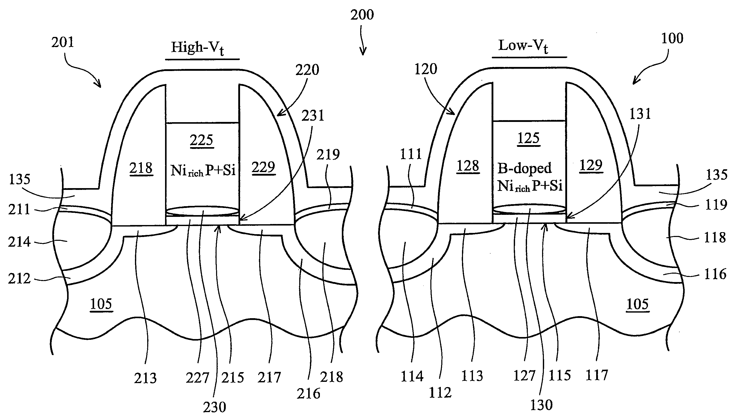
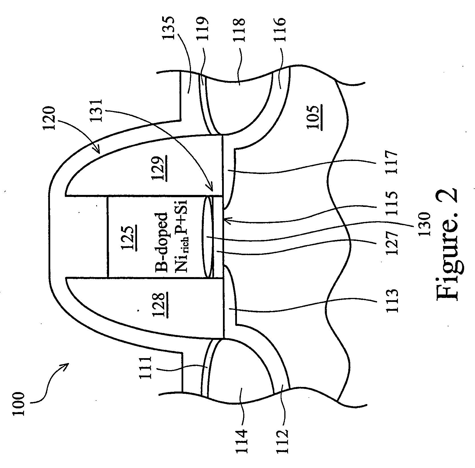
[0024]The present invention will be described with respect to preferred embodiments in a specific context, namely a PMOS device having a nickel-rich fully silicided (FUSI) metal gate. A nickel-rich FUSI metal gate is one in which substantially all of the original poly has been consumed in the silicidation process, and where the resulting gate electrode material has more nickel than silicon. The invention may also be applied, however, to PMOS devices made of similar material as well. The PMOS device may, for example, be one of the transistors in a CMOS (complementary metal-oxi...


PUM


Abstract

A PMOS (p-channel metal oxide semiconductor) device having at low voltage threshold MOSFET (MOS field effect transistor) with an improved work function and favorable DIBL (drain-induced barrier lowering) and SCE (short channel effect) characteristics, and a method for making such a device. The PMOS device includes a gate structure that is disposed on a substrate and includes a silicided gate electrode. The silicide is preferably nickel-rich and includes a peak platinum concentration at or near the interface between the gate electrode and a dielectric layer that separates the gate electrode from the substrate. The platinum peak region is produced by a multi-step rapid thermal annealing or similar process. The PMOS device may also include two such MOSFETs, one of which is boron-doped and one of which is not.

Description

TECHNICAL FIELD[0001]The present invention relates generally to the field of semiconductor devices, and more particularly relates to a PMOS device having a fully-silicided metal gate that may be used advantageously, for example in a multi-threshold IC (integrated circuit) application, and to a method for fabricating such a device.BACKGROUND[0002]Small electronic appliances are today used in a wide variety of applications and have become a ubiquitous part of modern society. These applications include computers, telephones, and home entertainment system components, among many others. One reason for the widespread use of these appliances is that recent advances in technology have expanded their capabilities while at the same time lowering their cost. A key part of this advancing technology has been the development of improved semiconductor devices and the processes for making them.[0003]Semiconductors are materials that after being properly treated conduct electricity when placed under...

Claims


Application Information

Patent Timeline
IPC IPC(8): H01L27/088H01L29/78
CPCH01L21/28097H01L21/82345H01L27/088H01L29/4975H01L29/66545H01L29/7833
Inventor TSAI, CHING-WEIWANG, CHIH-HAOLIN, WEI-JUNGHUANG, HUAN-TSUNGDIAZ, CARLOS H.
Owner TAIWAN SEMICON MFG CO LTD
Why Eureka
Try Eureka