Signaling circuit and method for integrated circuit devices and systems

a technology of integrated circuit devices and signals, applied in the direction of generating/distributing signals, instruments, pulse techniques, etc., can solve the problems of timing failures and power consumption timing failures can also aris

a technology of integrated circuit devices and signals, applied in the direction of generating/distributing signals, instruments, pulse techniques, etc., can solve the problems of timing failures and power consumption timing failures can also aris

US20080238519A1Inactive Publication Date: 2008-10-02DSM SOLUTIONS

Image

  • Signaling circuit and method for integrated circuit devices and systems
  • Signaling circuit and method for integrated circuit devices and systems
  • Signaling circuit and method for integrated circuit devices and systems

Examples


Embodiment Construction

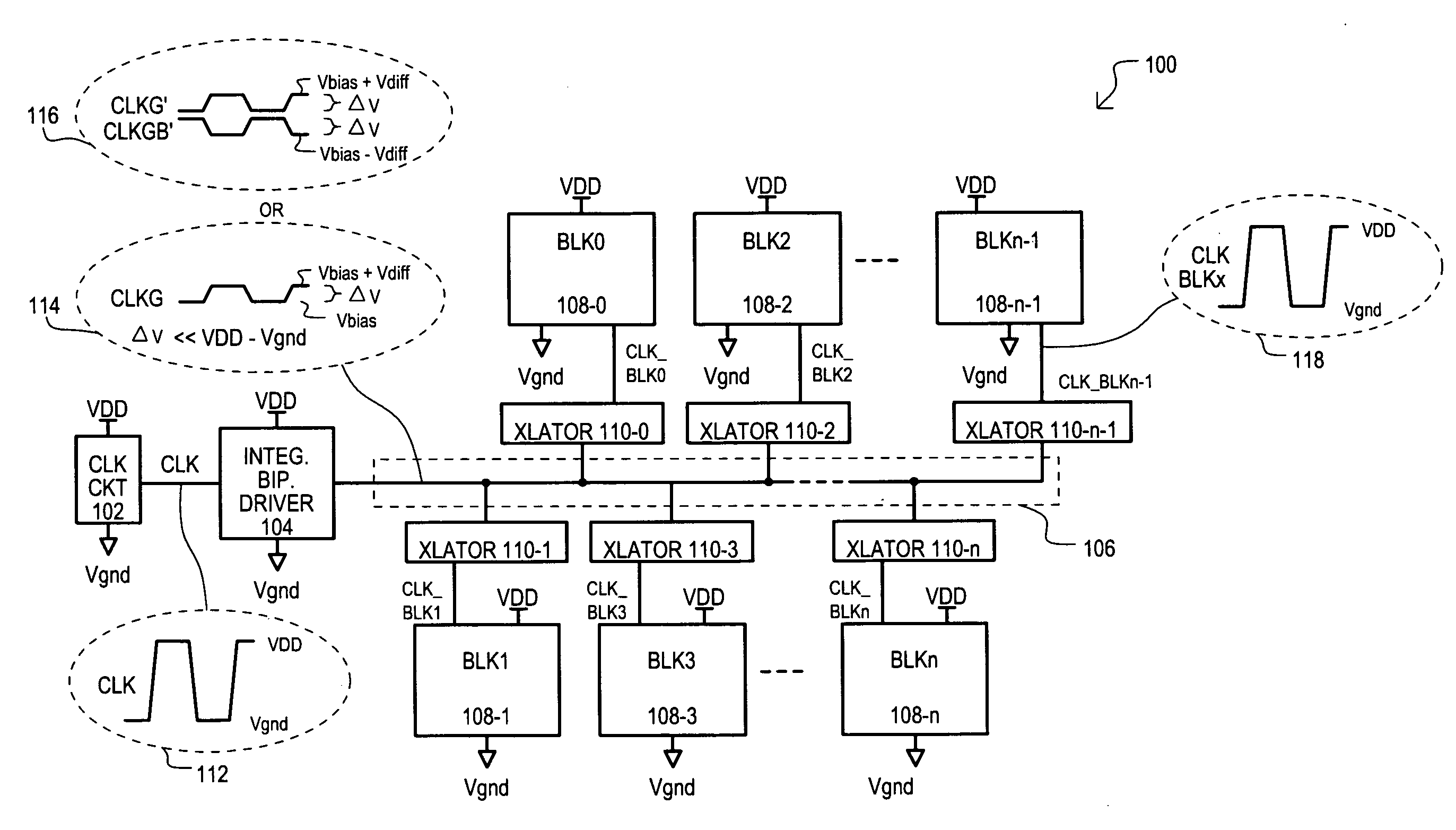
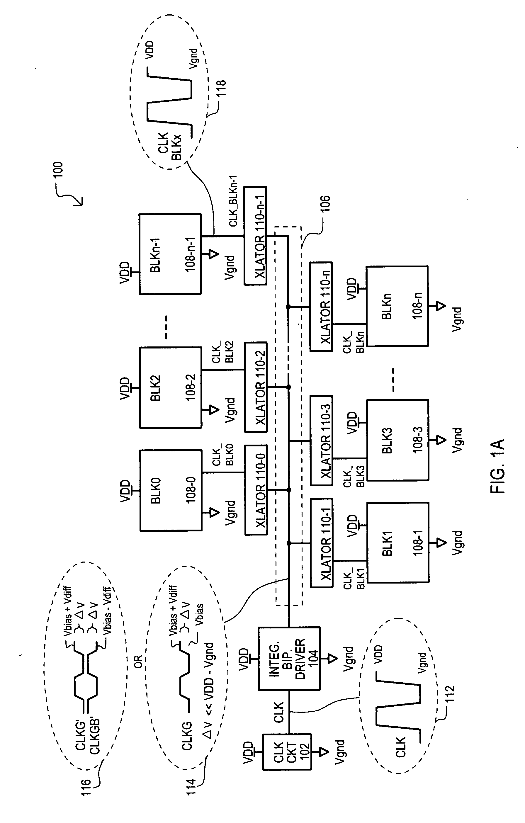
[0042]Various embodiments of the present invention will now be described in detail with reference to a number of drawings. The embodiments show structures, designs, and methods for an integrated circuit (IC) device that can consume less power and / or interfere less with other signals in the same IC device than conventional approaches, like those of complementary metal oxide semiconductor (CMOS) type ICs. Various embodiments can include bipolar transistors formed in the same integrated circuit as other transistors types, preferably in the same substrate as field effect transistors (FETs).

[0043]Referring now to FIG. 1A, an IC according to a first embodiment is shown in a block schematic diagram, and designated by the general reference character 100. An IC 100 can include a signal source circuit 102, a global transmitter circuit 104, a global wiring network 106, and a number of circuit blocks 108-0 to 108-n. Each circuit block (108-0 to 108-n) can be connected to global wiring network 1...


PUM


Abstract

Integrate circuit systems and semiconductor devices for generating, transmitting, receiving, and manipulating clock and / or data signals. A semiconductor device including a clock circuit having field effect transistors and a clock driver circuit having bipolar junction transistors is disclosed. The clock circuit may provide a first clock output having a first voltage swing. The clock driver circuit may receive the first clock output and provide a second clock output having a second voltage swing substantially less than the first voltage swing. The field effect transistors can be junction field effect transistors or insulated gate field effect transistors, or the like. The system / devices further including a translator circuit, for translating signals with a lower voltage swing into signals with a higher voltage swing, and a circuit block, for operating at such higher voltage swing. Further included are global and local wiring networks for communicating the signals between and among the individual circuits or system components.

Description

TECHNICAL FIELD[0001]The present invention relates generally to semiconductor integrated circuit devices, and more particularly to circuits and methods for transmitting, receiving and distributing signals on an integrated circuit and systems including integrated circuits.BACKGROUND OF THE INVENTION[0002]Integrated circuit (IC) devices typically include a number of sections formed in one or more substrates that are electrically interconnected to one another. As operating speeds for such devices has increased, the transmission of electrical signals across ICs with predetermined timing has become source of many design concerns, including timing failures and power consumption. Timing failures can arise due to instability of power supply levels, including β€œvoltage droop” (a drop in a high power supply level) and / or β€œground bounce” (a rise in a low power supply level). Timing failures can also arise due to transmission line effects, which can generate reflections at a signal receiving end...

Claims


Application Information

Patent Timeline
02 Oct 2008
Publication
US20080238519A1
IPC
H03K3/26; G06F17/50
CPC
G06F1/04; G06F1/10; G06F1/32; G06F17/5031; G06F30/3312
Inventors
KAPOOR, ASHOK KUMAR